Solid-state imaging device

a solid-state imaging and imaging element technology, applied in the direction of radio frequency controlled devices, instruments, television systems, etc., can solve the problems of large parameter capacitance of signal transmission paths, degraded high-speed response properties, and element dampedness, so as to reduce the damping of the waveform of the signal output of solid-state imaging elements and improve the high-speed response properties. , the effect of small parameter capacitan

Active Publication Date: 2012-08-14
HAMAMATSU PHOTONICS KK
View PDF18 Cites 0 Cited by
  • Summary
  • Abstract
  • Description
  • Claims
  • Application Information

AI Technical Summary

Benefits of technology

[0005]The present invention has been accomplished in view of the above point and an object of the invention is to provide a solid-state imaging apparatus, with which the parasitic capacitance of signal transmission paths is reduced to enable restraining of the damping of the waveforms of signals output from a solid-state imaging element and improvement of the high-speed response properties.
[0007]In the solid-state imaging apparatus according to the present invention, since the signal processing circuit is positioned at a planar portion of the package that differ from a planar portion at which the solid-state imaging element is positioned, the solid-state imaging element and the signal processing circuit are positioned proximally with respect to each other. Signal transmission path from the solid-state imaging element to the signal processing circuit is thereby made short and the parasitic capacitance of the signal transmission path is made small. As a result, the damping of the waveforms of the signal output from the solid-state imaging element can be restrained and the high-speed response properties can be improved.
[0009]In the solid-state imaging apparatus according to the present invention, the signal processing circuit is positioned proximally to the solid-state imaging element by making use of the step difference between the first planar portion and the second planar portion. Signal transmission path from the solid-state imaging element to the signal processing circuit is thereby made short and the parasitic capacitance of the signal transmission path is made small. As a result, the damping of the waveforms of the signal output from the solid-state imaging element can be restrained and the high-speed response properties can be improved.
[0010]As described above, by each of the solid-state imaging apparatuses according to the present invention, the solid-state imaging apparatus is provided with which the parasitic capacitance of the signal transmission path is reduced to enable restraining of the damping of the waveforms of the signal output from the solid-state imaging element and improvement of the high-speed response properties.
[0011]Preferably, the signal processing circuit includes a load resistor that is electrically connected to an output terminal of the solid-state imaging element. With the composition, since the solid-state imaging element and the load resistor are positioned apart from each other, even if the load resistor generate heat, adverse effects on the characteristics of the solid-state imaging element (for example, increasing of the dark current) can be prevented.
[0012]Also preferably, the signal processing circuit includes a load resistor, with which one end is electrically connected to an output terminal of the solid-state imaging element and the other end is grounded, and a buffer amplifier, having a bipolar transistor that is electrically connected to the output terminal of the solid-state imaging element. With the composition, since the solid-state imaging element and the load resistor are positioned apart from each other, even if the load resistor generates heat, adverse effects on the characteristics of the solid-state imaging element (for example, increasing of the dark current) can be prevented. Also, since the bipolar transistor is high in driving ability with respect to the load resistor, effects due to the parasitic capacitance of the signal transmission path subsequent the buffer amplifier can be alleviated.

Problems solved by technology

However, when the signal processing circuits are disposed at the exterior of the package, the signal transmission paths (electrical wirings) from the solid-state imaging element to the signal processing circuits become long and the parasitic capacitance of the signal transmission paths becomes large.
As a result, the waveforms of the signals output from the solid-state imaging element become damped and high-speed response properties are degraded.

Method used


Image

  • Solid-state imaging device
  • Solid-state imaging device
  • Solid-state imaging device

Examples


first embodiment

[0026](First Embodiment)

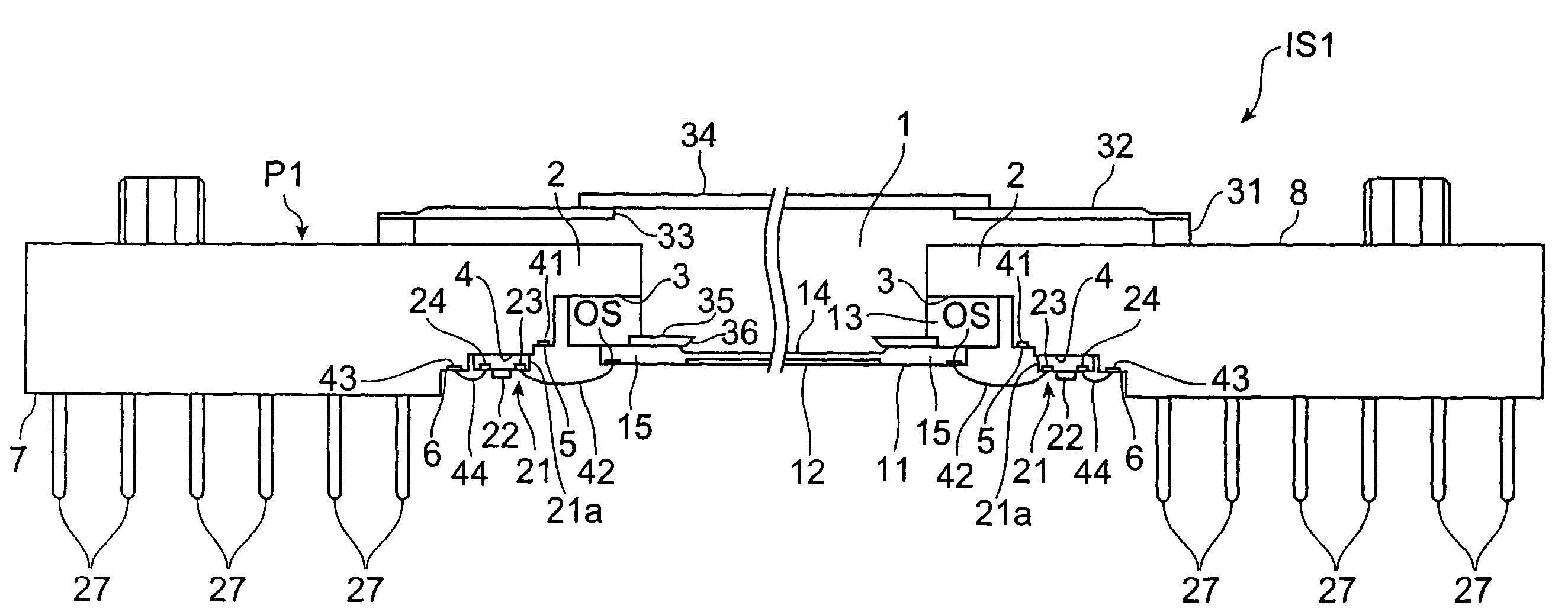
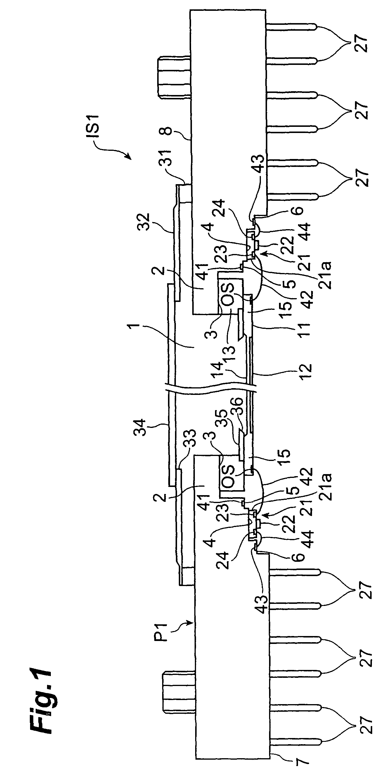
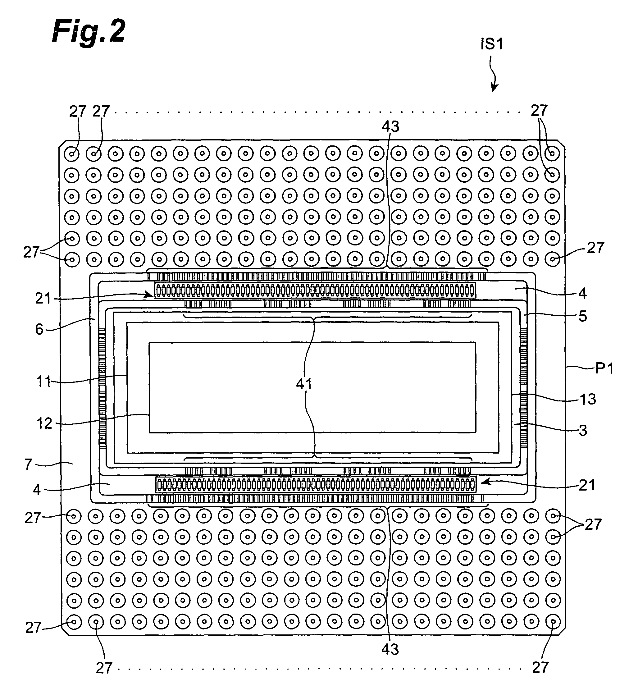
[0027]First, the composition of a solid-state imaging apparatus of a first embodiment shall be described based on FIGS. 1 to 3. FIG. 1 is a schematic view for describing the sectional composition of the solid-state imaging apparatus of the first embodiment. FIG. 2 is a plan view of the same solid-state imaging apparatus of the first embodiment. FIG. 3 is a circuit diagram for describing the composition of a signal processing circuit. FIG. 2 is a view viewed from a back surface (side opposite the side onto which energy rays are made incident) of the solid-state imaging apparatus.

[0028]A solid-state imaging apparatus IS1 of the first embodiment comprises a ceramic package P1, a back-illuminated CCD chip 11 (solid-state imaging element), chip resistor arrays 21, etc. At a central portion of package P1 is formed a hollow portion 1, which extends in a predetermined direction of package P1. In package P1, a mounting portion 2, for mounting CCD chip 11 and chip resi...

second embodiment

[0047](Second Embodiment)

[0048]The composition of a solid-state imaging apparatus of a second embodiment shall now be described based on FIGS. 5 to 8. FIG. 5 is a schematic view for describing the sectional composition of the solid-state imaging apparatus of the second embodiment. FIG. 6 is a plan view of the same solid-state imaging apparatus of the second embodiment. FIG. 7 is a plan view showing the composition of the vicinity of a buffer amplifier module. FIG. 8 is a circuit diagram for describing the composition of the buffer amplifier module. FIGS. 6 and 7 are diagrams of the solid-state imaging apparatus as viewed from the back surface side.

[0049]A solid-state imaging apparatus IS2 of the second embodiment comprises a package P2, CCD chip 11, buffer amplifier modules 61, which serve as signal processing circuits, etc.

[0050]Mounting portion 2 has a first planar portion 3 for positioning CCD chip 11, second planar portions 4 for positioning buffer amplifier modules 61, and a th...


PUM


Abstract

A solid-state imaging apparatuses IS1 comprises a package P1, a CCD chip 11, chip resistor arrays 21, etc. In package P1, a mounting portion 2, for mounting CCD chip 11 and chip resistor arrays 21, is disposed so as to protrude into a hollow portion 1. Mounting portion 2 has a first planar portion 3 and second planar portions 4, and first planar portion 3 and second planar portions 4 are formed to be stepped with respect to each other. CCD chip 11 is mounted and fixed on first planar portion 3 via a spacer 13. Chip resistor arrays 21 are mounted and fixed on second planar portions 4. Using the step difference between first planar portion 3 and second planar portions 4, CCD chip 11 and chip resistor arrays 21 are positioned proximally.

Description

TECHNICAL FIELD[0001]The present invention relates to a solid-state imaging apparatus.BACKGROUND ART[0002]There is known a solid-state imaging apparatus comprising: a solid-state imaging element, having an energy ray sensitive portion; and a package, housing the solid-state imaging element; and having signal processing circuits, which process signals output from the above-mentioned solid-state imaging element and are disposed at the exterior of the package (see, for example, Patent Document 1).[0003][Patent Document 1] Japanese Published Unexamined Patent Application No. H4-317280DISCLOSURE OF THE INVENTION[0004]However, when the signal processing circuits are disposed at the exterior of the package, the signal transmission paths (electrical wirings) from the solid-state imaging element to the signal processing circuits become long and the parasitic capacitance of the signal transmission paths becomes large. As a result, the waveforms of the signals output from the solid-state imagi...

Claims


Application Information

Patent Timeline
Patent Type & Authority Patents(United States)
IPC IPC(8): H04N3/14H04N5/335H01L27/14H04N5/361H04N5/372
CPCH01L27/14618H04N5/335H04N5/378H01L2924/15787H01L2224/48091H01L2924/1305H01L2924/19105H01L2924/05432H01L2924/00014H01L2924/00H04N25/00H04N25/75H01L27/146H01L27/14
Inventor KOBAYASHI, HIROYAAKAHORI, HIROSHIMURAMATSU, MASAHARU
Owner HAMAMATSU PHOTONICS KK
Why Eureka
Try Eureka