Photomultiplier

a multi-channel photomultiplier and electron transit time technology, applied in the field of photomultipliers, can solve the problems that the presence of stray photoelectrons cannot be ignored, and the average electron transit time difference cannot be improved, so as to improve the high-speed response properties of the multi-channel photomultiplier as a whole, reduce and improve the electron transit time difference in each electron multiplier

Inactive Publication Date: 2012-12-11
HAMAMATSU PHOTONICS KK
View PDF13 Cites 0 Cited by
  • Summary
  • Abstract
  • Description
  • Claims
  • Application Information

AI Technical Summary

Benefits of technology

[0008]The present inventors have examined the above conventional multichannel photomultiplier, and as a result, have discovered the following problems. That is, in the conventional multichannel photomultiplier, because electron multiplications are performed by electron multiplier channels that are allocated in advance according to positions of discharge of photoelectrons from the photocathode, positions of respective electrodes are designed optimally to reduce electron transit time differences according to each electron multiplier channel. By such improvement of the electron transit time differences in each electron multiplier channel, improvements are also made in the electron transit time differences of the multichannel photomultiplier as a whole and consequently, the high-speed response properties of the multichannel photomultiplier as a whole are improved.
[0011]The present invention has been developed to eliminate the problems described above. It is an object of the present invention to provide a photomultiplier that is significantly improved as a whole in such response time characteristics as TTS (transit time spread) and CTTD (cathode transit time difference) by realizing reduction of emission-position-dependent photoelectron transit time differences of photoelectrons emitted from a photocathode in a structure more suited for mass production.
[0015]In a conventional photomultiplier, the dynode pins are disposed along a periphery of the effective region of the electron multiplier section that avoids the effective region in which the dynodes are disposed and are specifically disposed along an outer periphery of a frame that supports the dynodes. Meanwhile, with the photomultiplier according to the present invention, because the dynode pins are disposed inside the effective region of the electron multiplier section, the effective region of the electron multiplier section can be enlarged as compared with the conventional photomultiplier. By enlargement of the effective region, trajectory modifications, especially of photoelectrons emitted from a periphery of the photocathode opposing the electron incidence surface of the electron multiplier section, are lessened in degree, and a focusing distance (transit distance of photoelectrons to arrival at the dynode unit of the first stage from the photocathode) is thus reduced significantly.
[0018]More specifically, the supporting frame of the n-th stage dynode unit preferably has an H shape formed by a pair of supports, disposed so as to sandwich all of the plurality of dynodes, and a connecting portion, having both ends fixed to the pair of supports and disposed so as to be sandwiched by at least two dynodes among the dynodes set to the same potential. Here, the connecting portion is provided with a structure to which one end of the associated dynode pin is fixed. Likewise, the insulating spacer, positioned between the n-th stage dynode unit and the (n+1)-th stage dynode unit (and constituting a part of the n-th stage dynode unit), has an H shape to secure a space for supporting the dynodes and a space for a dynode pin supporting structure. That is, the insulating spacer also has a pair of supports, associated to the pair of supports of the supporting frame in the n-th stage dynode unit, and a connecting portion, associated to the connecting portion of the supporting frame in the n-th stage dynode unit. By making the insulating spacer have the H shape, a space can be provided between dynode units even when the dynode units are respectively stacked in closely contacting states, thereby enabling evacuation to be performed readily in a manufacturing process and enabling an alkali metal vapor to be supplied adequately from the photocathode to the respective dynode units. The alkali metal vapor means as a material gas for forming the photocathode and a secondary electron emitting surface of each dynode.
[0022]Also, the insulating spacer, positioned between the n-th stage dynode unit and (n+1)-th stage dynode unit, may have a plurality of light shielding portions arranged so as to plaster the openings sandwiched by the dynodes in the n-th stage dynode unit. Here, each of the light shielding portions has a plurality slits each letting an alkali metal vapor pass therethrough. The light shielding portions, provided in the insulating spacers positioned between the stacked dynode units, functions to prevent that light generated in the anode side reaches the photocathode side, and the slits make an alkali metal vapor for photocathode formation pass from the anode side to the photocathode side.

Problems solved by technology

However, in such a multichannel photomultiplier, no improvements have been made in regard to the spread of the average electron transit time differences among the electron multiplier channels.
The presence of such stray photoelectrons cannot be ignored for further improvement of high-speed response properties.

Method used


Image

  • Photomultiplier
  • Photomultiplier
  • Photomultiplier

Examples


Embodiment Construction

[0049]In the following, embodiments of a photomultiplier according to the present invention will now be explained in detail with reference to FIGS. 1, 2A and 2B, 3 to 6, 7A to 12B, 13, 14A to 16B, 17, and 18A to 24B, respectively. In the description of the drawings, portions and elements that are the same shall be provided with the same symbol, and overlapping description shall be omitted.

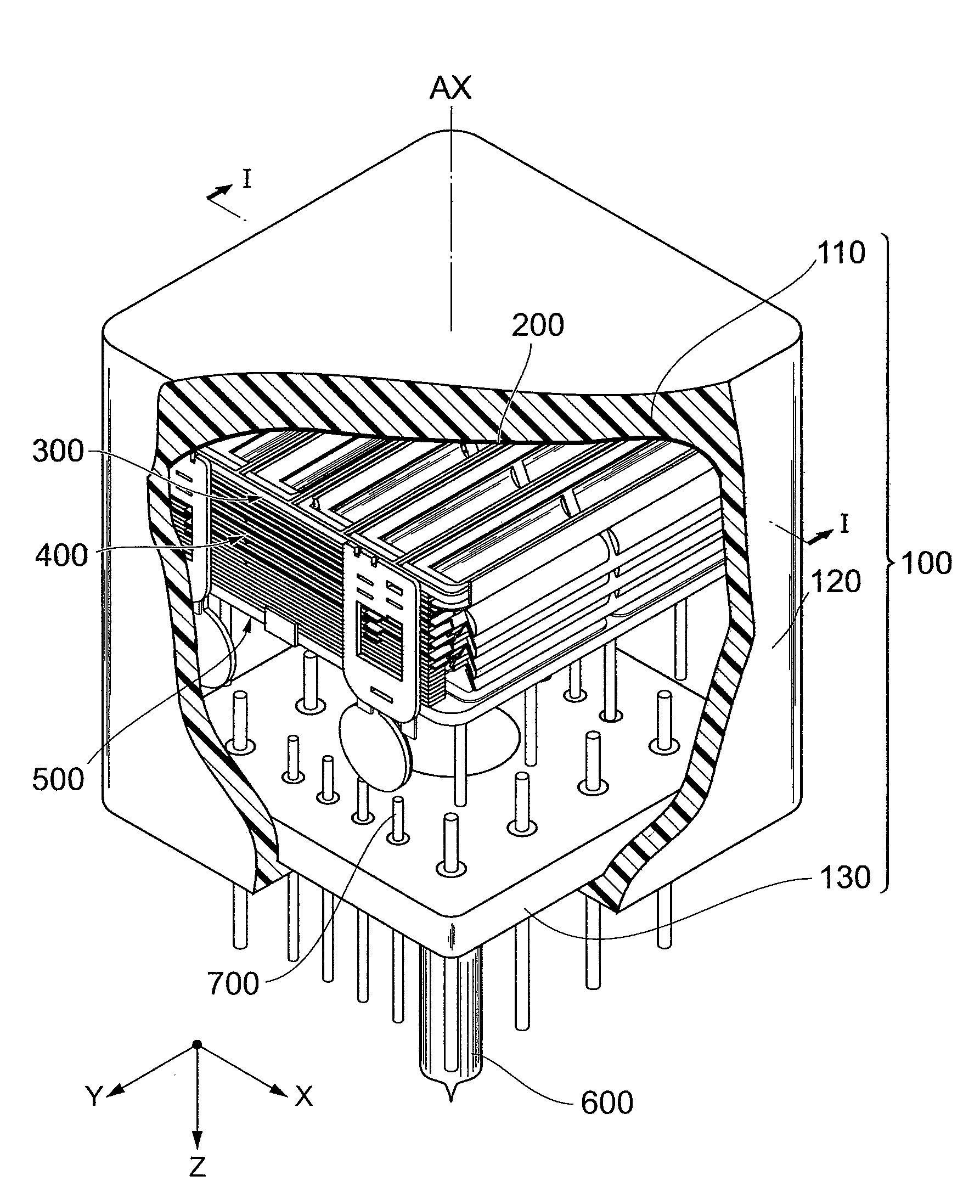
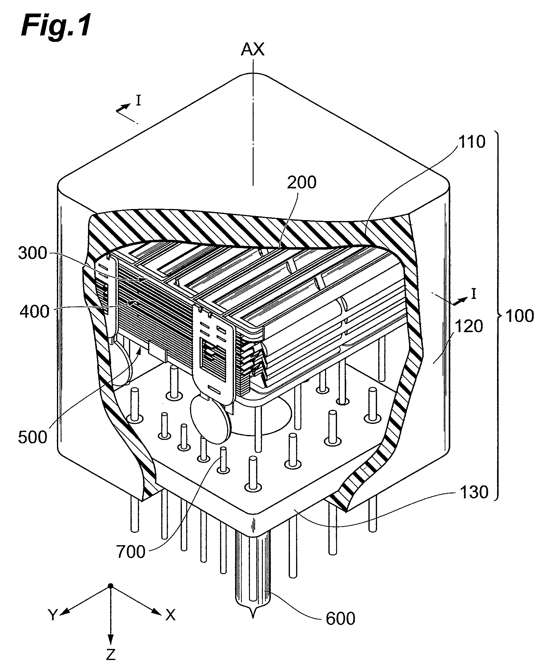
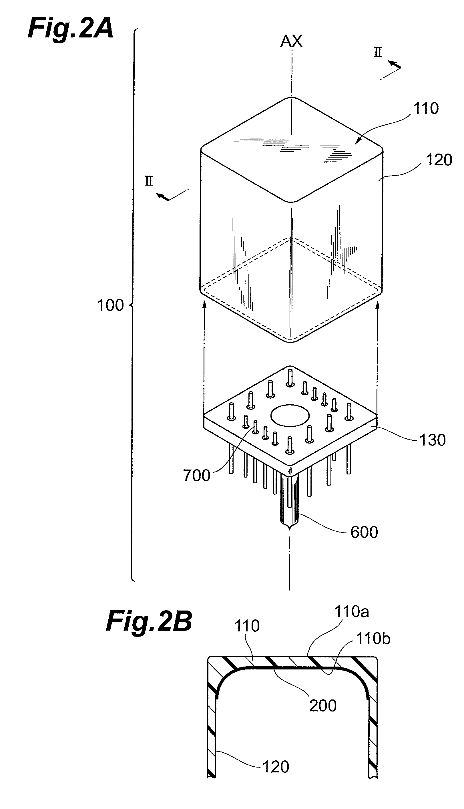
[0050]FIG. 1 is a partially broken-away view of a general configuration of an embodiment of a photomultiplier according to the present invention. FIGS. 2A and 2B are an assembly process diagram and a sectional view for describing a structure of a sealed container in the photomultiplier according to the present invention. FIG. 3 is a diagram of a sectional structure taken on line I-I of the photomultiplier shown in FIG. 1.

[0051]As shown in FIG. 1, the photomultiplier according to the present invention comprises a sealed container 100, having a pipe 600, used to depressurize an interior of the sealed...


PUM


Abstract

The present invention relates to a photomultiplier that realizes a significant improvement of response time characteristics by a structure enabling mass production. The photomultiplier comprises a sealed container, and, in the sealed container, a photocathode, an electron multiplier section, and an anode are respectively disposed. The electron multiplier section includes multiple stages of dynode units, and each of the multiple stages of dynode units is fixed with one end of the associated dynode pin while being electrically connected thereto. In particular, the dynode pin, whose one ends are fixed to the multiple stages of dynode units, are held within an effective region of the electron multiplier section contributing to secondary electron multiplication, when the electron multiplier section is viewed from the photocathode side. By this configuration, a focusing distance from the photocathode to a first stage dynode unit can be shortened effectively and the effective region of the electron multiplier section can be enlarged to effectively reduce variations in transit time of photoelectrons propagating from the photocathode to the first stage dynode unit.

Description

CROSS-REFERENCE TO RELATED APPLICATION[0001]This application claims priority to Provisional Application No. 61 / 030,364 filed on Feb. 21, 2008 by the same Applicant, which is hereby incorporated by reference in its entirety.BACKGROUND OF THE INVENTION[0002]1. Field of the Invention[0003]The present invention relates to a photomultiplier capable of successively emitting secondary electrons in multiple stages in response to incidence of photoelectrons from a photocathode and thereby performing cascade multiplication of the secondary electrons.[0004]2. Related Background Art[0005]The development of TOF-PET (time-of-flight PET) as a next-generation PET (positron emission tomography) apparatus is being pursued actively in the field of nuclear medicine in recent years. In a TOF-PET apparatus, because two gamma rays, emitted from a radioactive isotope administered into a body, are measured simultaneously, a large number of photomultipliers having excellent, high-speed response properties ar...

Claims


Application Information

Patent Timeline
Patent Type & Authority Patents(United States)
IPC IPC(8): H01J43/18
CPCH01J43/26H01J43/28
Inventor OHMURA, TAKAYUKIKYUSHIMA, HIROYUKISHIMOI, HIDEKIKODAMA, TSUYOSHI
Owner HAMAMATSU PHOTONICS KK
Why Eureka
Try Eureka