Photomultiplier

a multi-channel photomultiplier and electron multiplier technology, applied in the field of photomultipliers, can solve the problems of inability to ignore the presence of such stray photoelectrons, the inability to improve the spread of average electron transit time differences among the electron multiplier channels, so as to improve the high-speed response properties of the whole multi-channel photomultiplier, the effect of reducing electron transit time differences

Inactive Publication Date: 2010-02-09
HAMAMATSU PHOTONICS KK
View PDF24 Cites 0 Cited by
  • Summary
  • Abstract
  • Description
  • Claims
  • Application Information

AI Technical Summary

Benefits of technology

[0008]The present inventors have examined the above prior art, and as a result, have discovered the following problems. That is, in the conventional multichannel photomultiplier, because electron multiplications are performed by electron multiplier channels that are allocated in accordance with release positions of photoelectrons from the photocathode, the positions of the respective electrodes are designed optimally so as to reduce electron transit time differences according to each electron multiplier channel. In this manner, by such improvement of the electron transit time differences in each electron multiplier channel, improvements are made in the electron transit time differences of the whole multichannel photomultiplier and consequently, the high-speed response properties of the whole multichannel photomultiplier are improved.
[0011]The present invention has been developed to eliminate the problems described above, and an object thereof is to realize a gain control for every electron multiplier channel by a structure more suited for mass production to provide a photomultiplier that is significantly improved as a whole in such response time properties as TTS (Transit Time Spread) and CTTD (Cathode Transit Time Difference).
[0020]Also, in order to realize highly precise gain control according to each electron multiplier channel, the photomultiplier may have a structure that effectively reduces the crosstalk between the electron multiplier channels. Specifically, a partitioning plate that partitions the second dynode in two in the longitudinal direction of the second dynode is provided. The second dynode is set to a higher potential than the first dynode that emits secondary electrons according to the incidence of photoelectrons from the cathode and is arranged at a position at which the secondary electrons from the first dynode arrives. By the partitioning plate arranged inside the second dynode, crosstalk between mutually adjacent electron multiplier channels constituted by one dynode set can be reduced effectively. That is, the trajectories of electrons that propagate successively along the plurality of stages of dynodes are significantly reduced in the possibility of crossing across to adjacent electron multiplier channels in this process (the crosstalk between adjacent electron multiplier channels is reduced significantly).

Problems solved by technology

However, in such a multichannel photomultiplier, no improvements had been made in regard to the spread of the average electron transit time differences among the electron multiplier channels.
The presence of such stray photoelectrons cannot be ignored for further improvement of high-response properties.
In addition, the presence of such stray photoelectrons is also a major cause of occurrence of crosstalk among electron multiplier channels.

Method used


Image

  • Photomultiplier
  • Photomultiplier
  • Photomultiplier

Examples


Embodiment Construction

[0031]In the following, embodiments of a photomultiplier according to the present invention will be explained in detail with reference to FIGS. 1, 2A-2B, 3-4, 5A-5B, 6, 7A, and 7B. In the explanation of the drawings, constituents identical to each other will be referred to with numerals identical to each other without repeating their overlapping descriptions.

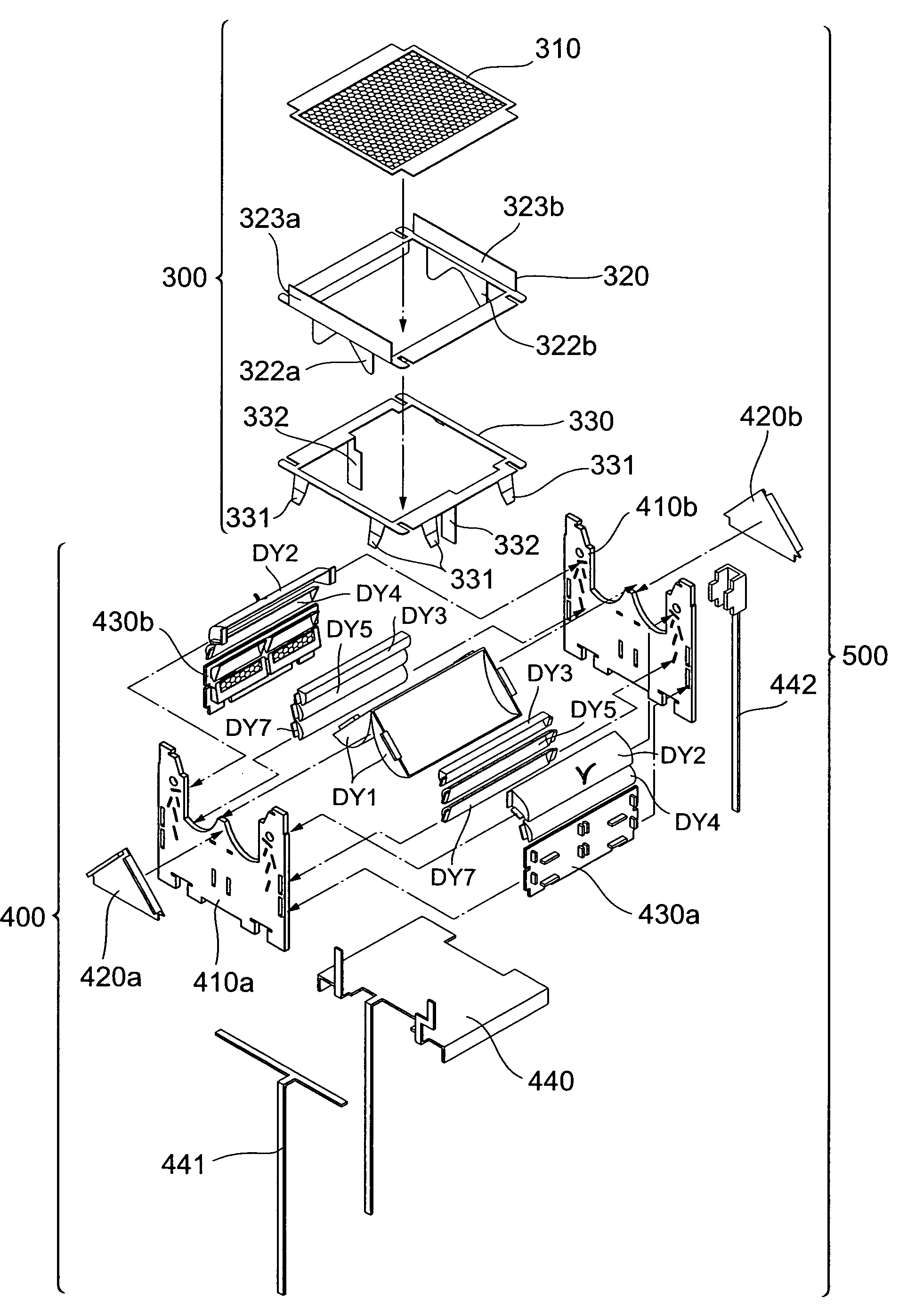
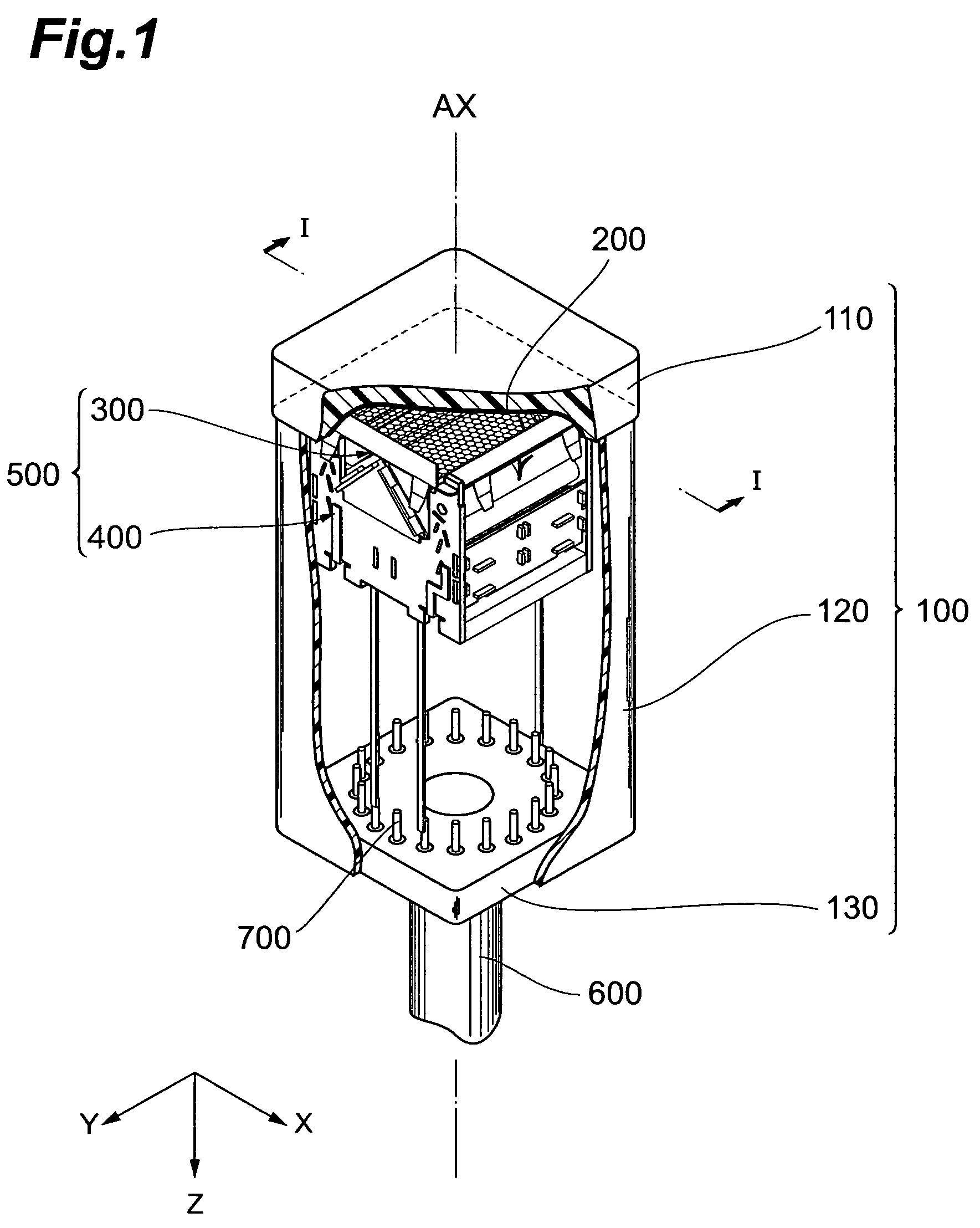
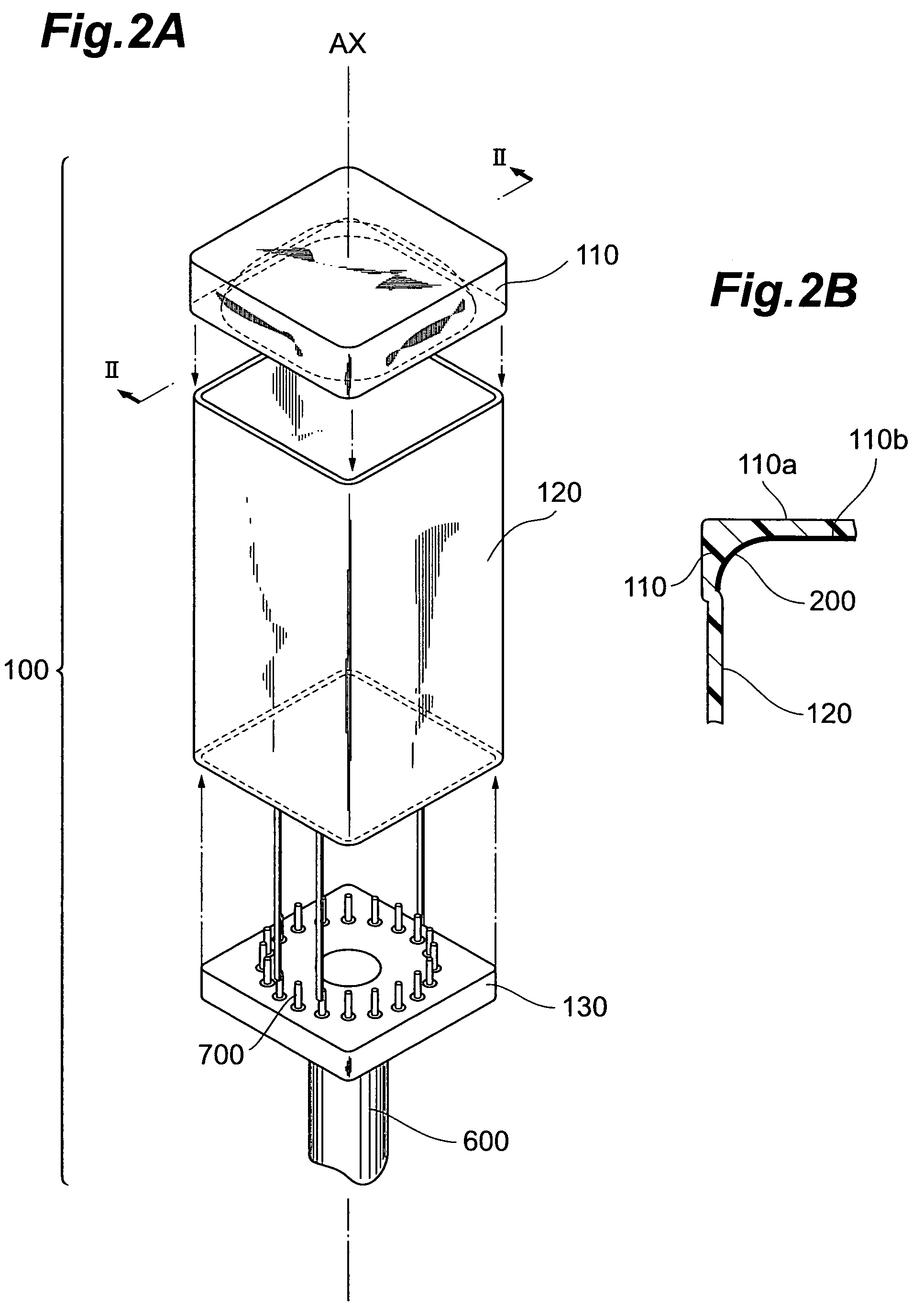
[0032]FIG. 1 is a partially broken-away view of a general arrangement of an embodiment of a photomultiplier according to the present invention. FIGS. 2A and 2B are an assembly process diagram and a sectional view, respectively, for explaining a structure of a sealed container in the photomultiplier according to the present invention.

[0033]As shown in FIG. 1, the photomultiplier according to the present invention has a sealed container 100, with a pipe 600, which is used to depressurize the interior to a predetermined degree of vacuum (and the interior of which is filled after vacuum drawing), provided at a bottom portion, and ha...


PUM


Abstract

The present invention relates to a photomultiplier that realizes significant improvement of response time properties with a structure enabling mass production. The photomultiplier comprises a sealed container, and, in the sealed container, a photocathode, at least one dynode set, a dynode unit including a part of insulating supporting members holding the one dynode unit, and a gain control unit are housed. The gain control unit has an insulating base plate, and the insulating base plate is integrally fixed with a control dynode and a final stage dynode that belong to each dynode set together with an anode. By the insulating base plate thus being clamped by the pair of insulating supporting members, the anode, the control dynode, and the final stage dynode constitute a part of an electron multiplier section.

Description

CROSS-REFERENCE TO RELATED APPLICATION[0001]This application claims priority to U.S. Provisional Application Ser. No.: 60 / 851,751 filed on Oct. 16, 2006 by the same Applicant, which is hereby incorporated by reference in its entirety.BACKGROUND OF THE INVENTION[0002]1. Field of the Invention[0003]The present invention relates to a photomultiplier, which, in response to incidence of photoelectrons, can perform cascade multiplication of secondary electrons by successive emission of the secondary electrons in multiple stages.[0004]2. Related Background Art[0005]In recent years, development of TOF-PET (Time-of-Flight PET) as a next-generation PET (Positron Emission Tomography) device is being pursued actively in the field of nuclear medicine. In a TOF-PET device, because two gamma rays, emitted from a radioactive isotope administered into a body, are measured simultaneously, a large number of photomultipliers with excellent, high-speed response properties are used as measuring devices t...

Claims


Application Information

Patent Timeline
Patent Type & Authority Patents(United States)
IPC IPC(8): H01J43/20
CPCH01J43/26
Inventor OHMURA, TAKAYUKIYAMAGUCHI, TERUHIKO
Owner HAMAMATSU PHOTONICS KK
Why Eureka
Try Eureka