Light-emitting element, light-emitting device, and electronic device

a light-emitting device and light-emitting element technology, applied in the direction of thermoelectric device junction materials, semiconductor devices, electrical apparatus, etc., can solve the problem of difficult to strike the carrier balance between electrons and holes with a single material, and achieve good carrier balance, high emission efficiency, and easy fabrication

Active Publication Date: 2012-08-21
SEMICON ENERGY LAB CO LTD
View PDF102 Cites 13 Cited by
  • Summary
  • Abstract
  • Description
  • Claims
  • Application Information

AI Technical Summary

Benefits of technology

[0020]However, as a result of intense study, the present inventors have found that even with a single film containing a single substance, the carrier balance can be improved by adding a carrier-trapping substance to an appropriate position of the film. The present inventors have found that this find can be used to solve the aforementioned problem without forming a heterostructure by applying an element structure as described below.
[0025]Here, although the above-described light-emitting element has a structure in which the carrier balance in the organic compound film including the first organic compound is improved, injection of carriers from the electrodes to the organic compound film is also important in enabling the light-emitting element to emit light more efficiently. Balance of this injection from the electrodes is important also in terms of lifetime since a change in carrier balance over time leads to luminance decay.
[0034]In recent years, a technique in which a full color display can be fabricated by providing a white light-emitting element with color filters has been proposed. A feature of such a technique is simplicity with which a full color display can be fabricated by forming just a white light-emitting element over a substrate. Thus, a light-emitting element of the embodiment of the present invention which can be easily fabricated is applied to a white light-emitting element, which is combined with color filters; accordingly, the effect of reducing costs can be obtained at the same time.
[0039]By applying the present invention, a light-emitting element with a good carrier balance can be fabricated without forming a heterostructure. Accordingly, a light-emitting element with high emission efficiency which is easily fabricated can be provided.
[0040]Further, by applying the present invention, a light-emitting element in which a variation in carrier balance over time is small can be fabricated without forming a heterostructure. Accordingly, a light-emitting element with long lifetime can be provided.
[0041]Furthermore, by using the present invention, a light-emitting device with low power consumption and long lifetime can be provided. Moreover, an electronic device with long lifetime can be provided.

Problems solved by technology

In an organic compound, however, since the hole-transport capability and the electron-transport capability are at different levels, the carrier balance between holes and electrons is difficult to strike with a single material.

Method used


Image

  • Light-emitting element, light-emitting device, and electronic device
  • Light-emitting element, light-emitting device, and electronic device
  • Light-emitting element, light-emitting device, and electronic device

Examples


embodiment 1

[0093]In Embodiment 1, the concept and basic structure of the embodiment of the present invention will be described with reference to materials and fabrication methods which are used.

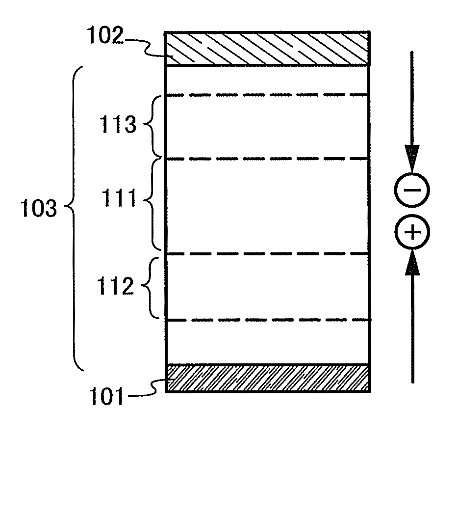
[0094]First, a case is considered where an organic compound film provided between an anode and a cathode contains a single organic compound (hereinafter, referred to as a first organic compound) and where a light-emitting substance is added to the organic compound film in order to control a light-emitting region and an emission color. This light-emitting region to which the light-emitting substance is added is preferably away from the anode and from the cathode so as to prevent quenching due to the electrode.

[0095]Many of organic compounds enable both holes and electrons to flow therethrough in a thin film state. In other words, in many cases, even a material that is generally called a hole-transport material enables electrons to flow therethrough, whereas even a material called an electron-transport ma...

embodiment 2

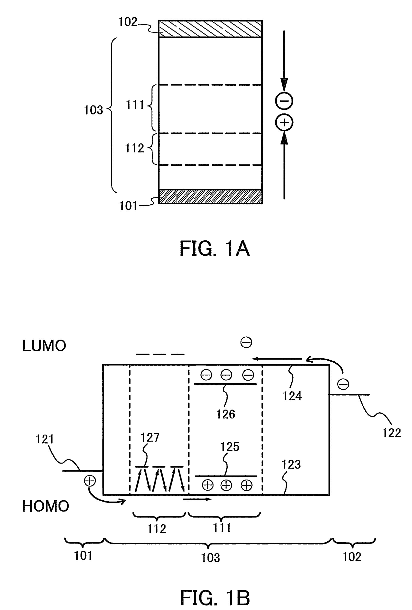
[0149]In Embodiment 2, another structure of an embodiment of the present invention which is obtained by development of the basic structure disclosed in Embodiment 1 will be described using FIGS. 4A and 4B and FIG. 5.

[0150]FIGS. 4A and 4B and FIG. 5 each illustrate a light-emitting element of an embodiment of the present invention which includes the organic compound film 103 containing the first organic compound between the anode 101 and the cathode 102; the organic compound film 103 is provided in contact with the anode 101 and with the cathode 102. Thus, the organic compound film 103 includes the light-emitting region to which the light-emitting substance is added and further includes the hole-transport region to which the hole-trapping substance is added and / or the electron-transport region to which the electron-trapping substance is added. The structures of these light-emitting region, hole-transport region, and electron-transport region are as disclosed in Embodiment 1.

[0151]In ...

embodiment 3

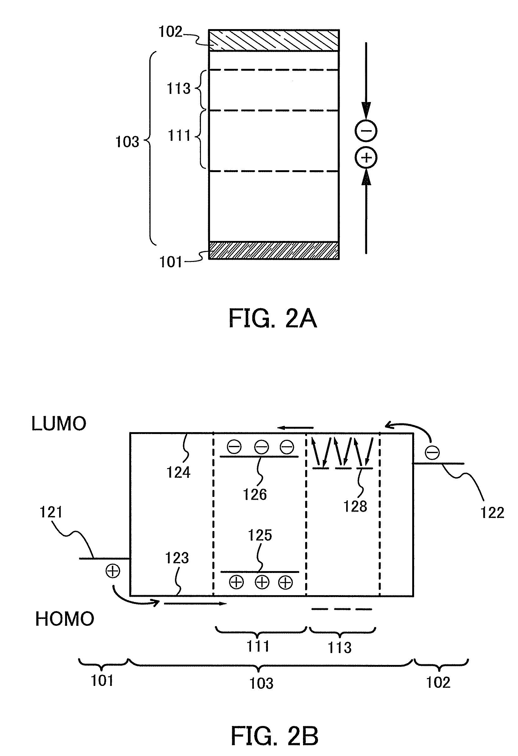
[0162]In Embodiment 3, another structure of an embodiment of the present invention which is obtained by development of the basic structure disclosed in Embodiment 1 will be described using FIGS. 6A and 6B and FIG. 7.

[0163]FIGS. 6A and 6B and FIG. 7 each illustrate a light-emitting element of an embodiment of the present invention which includes the organic compound film 103 containing the first organic compound between the anode 101 and the cathode 102, wherein the organic compound film 103 is provided in contact with the anode 101 and with the cathode 102. Thus, the organic compound film 103 includes the light-emitting region to which the light-emitting substance is added and further includes a hole-transport region to which a hole-trapping substance is added and / or an electron-transport region to which an electron-trapping substance is added. The structures of these light-emitting region, hole-transport region, and electron-transport region are similar to those disclosed in Embodi...


PUM


Abstract

Disclosed is a light-emitting element with a good carrier balance and manufacturing method thereof which does not require the formation of the heterostructure. The light-emitting element includes an organic compound film containing a first organic compound as the main component (base material) between an anode and a cathode, wherein the organic compound film is provided in contact with the anode and with the cathode. The first organic compound further includes a light-emitting region to which a light-emitting substance is added and includes a hole-transport region to which a hole-trapping substance is added and / or an electron-transport region to which an electron-trapping substance is added. The hole-transport region is located between the light-emitting region and the anode, and the electron-transport region is located between the light-emitting region and the cathode.

Description

TECHNICAL FIELD[0001]The present invention relates to a light-emitting element that employs electroluminescence. Further, the present invention relates to a light-emitting device and an electronic device each having the light-emitting element.BACKGROUND ART[0002]In recent years, research and development of light-emitting elements using electroluminescence (EL) have been extensively conducted. In the basic structure of such a light-emitting element, a light-emitting substance is interposed between a pair of electrodes. By applying a voltage to this element, light emission can be obtained from the light-emitting substance.[0003]Since this type of light-emitting element is a self-luminous type, it has advantages over a liquid crystal display in that visibility of a pixel is high and that no backlight is needed. Therefore, light-emitting elements are thought to be suitable as flat panel display elements. Further, such a light-emitting element also has advantages in that the element can ...

Claims


Application Information

Patent Timeline
Patent Type & Authority Patents(United States)
IPC IPC(8): H01L51/52
CPCH01L51/5203H01L51/5052H01L51/006H01L51/0061H01L51/0072H01L51/5088H01L51/5092H01L51/0085H10K85/636H10K85/633H10K85/342H10K85/6572H10K50/17H10K50/171H10K50/155H10K50/165H10K50/805H10K50/11
Inventor SEO, SATOSHIOHSAWA, NOBUHARU
Owner SEMICON ENERGY LAB CO LTD
Why Eureka
Try Eureka