Organic electroluminescent material, electronic component and electronic device

An electroluminescent material and luminescent technology, applied in luminescent materials, electrical components, organic chemistry, etc.

Active Publication Date: 2022-06-24
SHAANXI LIGHTE OPTOELECTRONICS MATERIAL CO LTD
View PDF7 Cites 0 Cited by
  • Summary
  • Abstract
  • Description
  • Claims
  • Application Information

AI Technical Summary

Problems solved by technology

[0003] In the existing organic electroluminescent devices, the most important problems are life and efficiency. With the increase of the area of ​​the display, the driving voltage is also increased, and the luminous efficiency and current efficiency also need to be improved. Therefore, it is necessary to continue to develop new types of electroluminescent devices. materials to further enhance the performance of organic electroluminescent devices

Method used


Image

  • Organic electroluminescent material, electronic component and electronic device
  • Organic electroluminescent material, electronic component and electronic device
  • Organic electroluminescent material, electronic component and electronic device

Examples


Embodiment 1

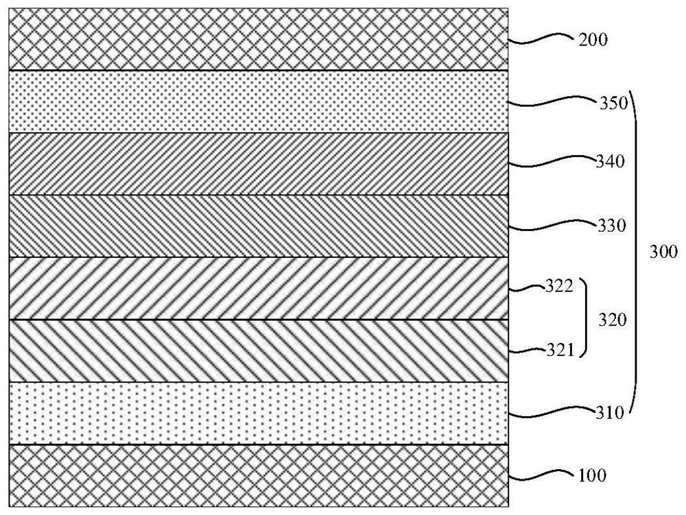
[0303] The anode is prepared by the following process: the thickness is The ITO substrate (manufactured by Corning) was cut into a size of 40mm × 40mm × 0.7mm, and a photolithography process was used to prepare it into an experimental substrate with patterns of cathodes, anodes and insulating layers, using ultraviolet ozone and O 2 :N 2 A plasma surface treatment was performed to increase the work function of the anode (experimental substrate) and to remove scum.

[0304] Vacuum evaporation of F4-TCNQ on the experimental substrate (anode) to form a thickness of The hole injection layer (HIL), and NPB was evaporated on the hole injection layer to form a thickness of the first hole transport layer.

[0305] PAPB was vacuum evaporated on the first hole transport layer to form a thickness of the second hole transport layer.

[0306] On the second hole transport layer, compound 1:GH-N:Ir(ppy) 3 Co-evaporation was performed at a ratio of 60:40:10% (co-evaporation rate rati...

Embodiment 2~ Embodiment 89

[0310] Organic electroluminescent devices were fabricated by the same method as in Example 1, except that the compounds shown in Table 11 were used instead of Compound 1 when forming the light-emitting layer.


PUM


Abstract

This application belongs to the technical field of organic materials, and provides a nitrogen-containing compound, an organic electroluminescence device and an electronic device, the structure of the nitrogen-containing compound is shown in Chemical Formula I,

Description

technical field [0001] The present application belongs to the technical field of organic materials, and in particular relates to an organic electroluminescent material, an electronic component and an electronic device. Background technique [0002] An organic electroluminescent device, such as an organic light emitting diode (OLED), generally includes a cathode and an anode disposed opposite to each other, and a functional layer disposed between the cathode and the anode. The functional layer is composed of multiple organic or inorganic film layers, and generally includes an organic light-emitting layer, a hole transport layer, an electron transport layer, and the like. When a voltage is applied to the cathode and anode, the two electrodes generate an electric field. Under the action of the electric field, the electrons on the cathode side move to the electroluminescent layer, and the holes on the anode side also move to the light-emitting layer, and the electrons and holes ...

Claims


Application Information

Patent Timeline
Patent Type & Authority Patents(China)
IPC IPC(8): C07D519/00C09K11/06H01L51/54H01L51/50
CPCC07D519/00C09K11/06C09K2211/1033C09K2211/1044C09K2211/1059C09K2211/1007C09K2211/1011C09K2211/1077C09K2211/1081C09K2211/1085H10K85/624H10K85/615H10K85/654H10K85/657H10K85/6576H10K85/6572H10K85/6574H10K50/11
Inventor 马天天徐先彬南朋
Owner SHAANXI LIGHTE OPTOELECTRONICS MATERIAL CO LTD
Why Eureka
Try Eureka