Method of manufacturing semiconductor device

a manufacturing method and semiconductor technology, applied in the direction of semiconductor devices, basic electric elements, electrical appliances, etc., can solve the problems of difficult ion implantation method to implant, inability to obtain desired threshold voltage, etc., and achieve the effect of improving reliability

Inactive Publication Date: 2012-08-28
RENESAS ELECTRONICS CORP
View PDF7 Cites 23 Cited by
  • Summary
  • Abstract
  • Description
  • Claims
  • Application Information

AI Technical Summary

Benefits of technology

[0018]Advantageous effects obtained by a typical preferred embodiment of a typical invention among those disclosed in the present application are to be described below.
[0019]In a semiconductor device having a FIN type transistor including a FIN-shape semiconductor portion, scattering of characteristics of the FIN type transistor can be suppressed, thereby improving the reliability by decreasing the difference between the impurity concentration at the upper surface and the impurity concentration on the lateral side of the FIN-shape semiconductor portion.DESCRIPTION OF THE ACCOMPANYING DRAWINGS
[0020]FIG. 1 is a perspective view for a main portion of a semiconductor substrate showing a manufacturing step of a FIN type transistor according to an

Problems solved by technology

However, it is difficult in the ion implantation method to implant impurity ions uniformly to the upper surface and the lateral sides of the FIN-shape semiconductor portion.
As a result, the impurity concentration at the upper surface of the FIN-shape semiconductor portion restricts the threshold voltage of the FIN type transistor to result in a problem that a desired threshold voltage cannot be obtained.

Method used


Image

  • Method of manufacturing semiconductor device
  • Method of manufacturing semiconductor device
  • Method of manufacturing semiconductor device

Examples


Embodiment Construction

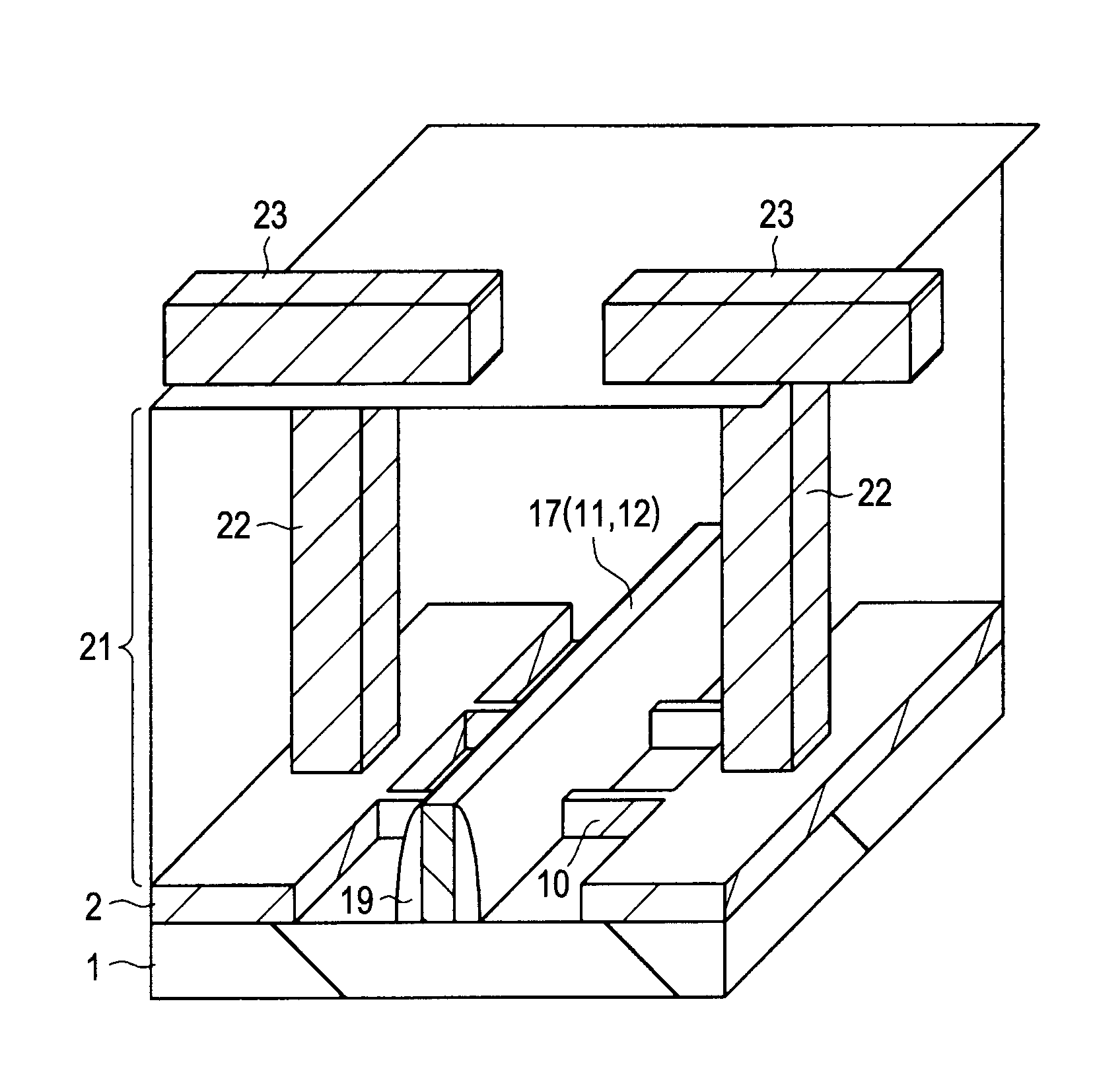
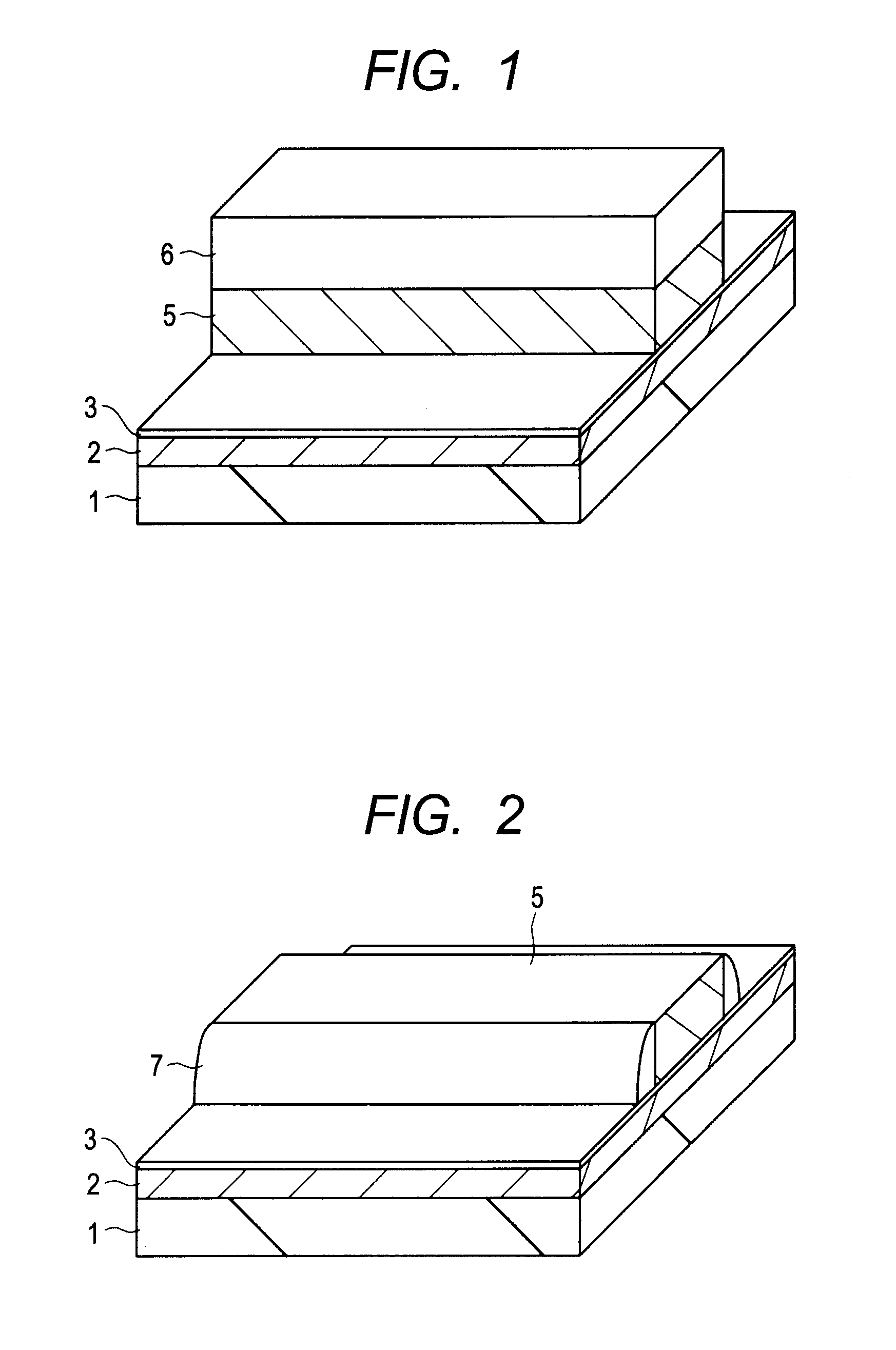
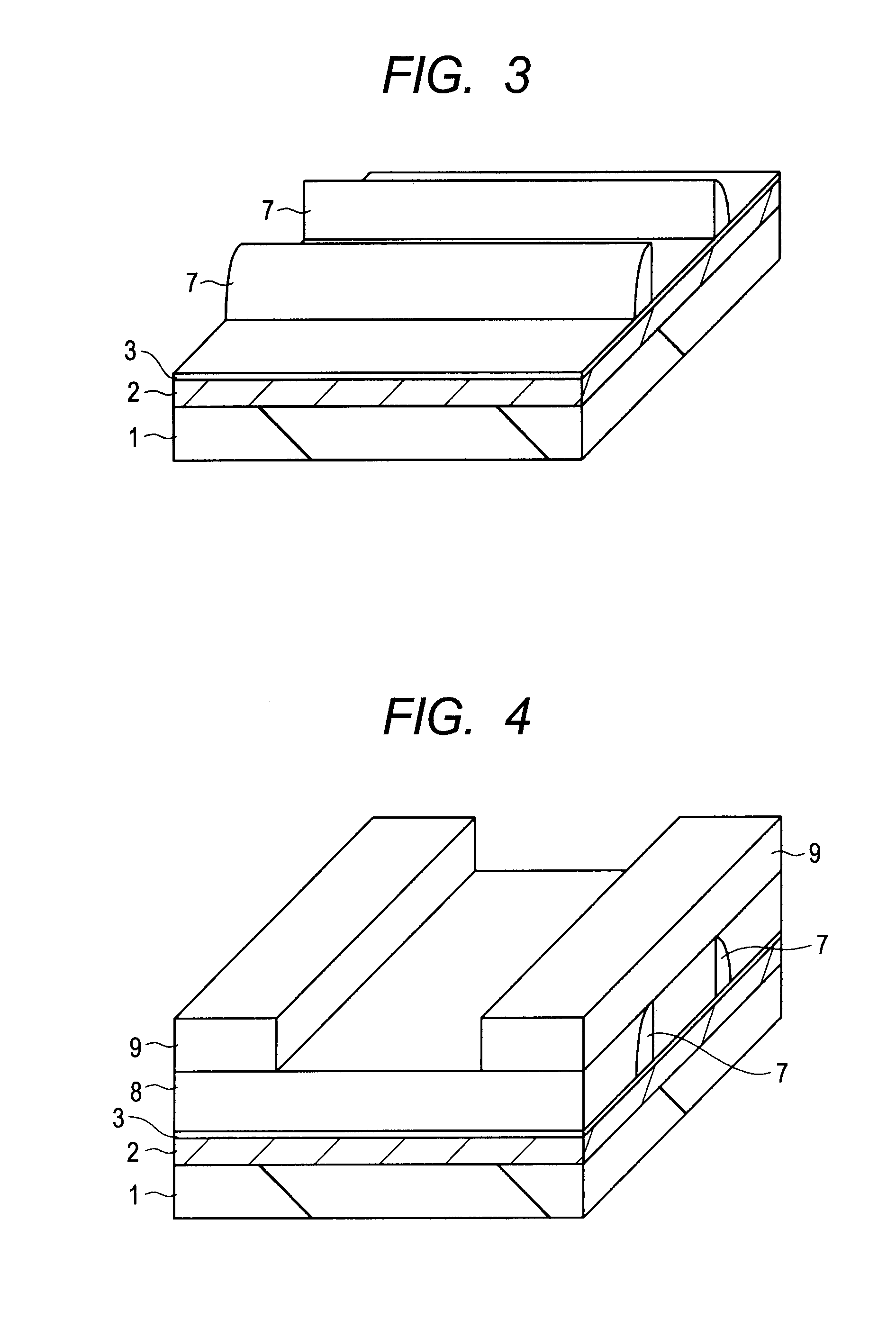
[0039]In the embodiments described hereinafter, when it is necessary for the sake of convenience, they may be explained while being divided into a plurality of sections or a plurality of embodiments. However, unless otherwise specified particularly, they are not irrelevant to each other, and there exists a relationship such that one embodiment is a modification, a detailed explanation or a complementary explanation of a portion or the whole of other embodiments.

[0040]Further, in the description of the embodiments hereinafter, when the reference is made to a specific number and the like (including number, numerical values, quantity, range and the like) of elements, unless otherwise specified and unless it is obvious that the number and the like of elements are definitely limited to the specific number in principle, the number and the like are not limited to such specific number and may be a number above or below the specific number. Further, in the description of the embodiments here...


PUM


Abstract

A semiconductor device having a FIN type transistor including a FIN-shape semiconductor portion improved for reliability by suppressing scattering of the characteristics of the FIN-shape transistor by decreasing a difference between impurity concentration at an upper surface and impurity concentration on a lateral side of the FIN-shape semiconductor portion, in which a pad insulating film at a thickness of about 2 to 5 nm is formed to the upper surface of the FIN-shape semiconductor portion, cluster ions are implanted to one lateral side of the FIN-shape semiconductor portion from an oblique direction at a first implantation angle θ1 and then cluster ions are implanted to another lateral side of the FIN-shape semiconductor portion from an oblique direction at a second implantation angle θ2 in symmetrical with the first implantation angle θ1 and, subsequently, the cluster ions implanted to the FIN-shape semiconductor portion 10 are activated to form a diffusion region that forms a portion of a source region and a drain region.

Description

CROSS-REFERENCE TO RELATED APPLICATIONS[0001]The disclosure of Japanese Patent Application No. 2010-62836 filed on Mar. 18, 2010 including the specification, drawings and abstract is incorporated herein by reference in its entirety.BACKGROUND OF THE INVENTION[0002]The present invention concerns a technique for manufacturing a semiconductor device and, more specifically, it relates to a technique which is effective when applied to the manufacture of a semiconductor device having a FIN type transistor including a FIN-shape semiconductor portion.[0003]For proceeding with the high integration degree of integrated circuits configuring semiconductor devices, refinement of transistors has been conducted. However, existent planar type transistors have confronted to physical limit, and development of a novel transistor structure other than that of the planar type has been necessary for the refinement of the transistors.[0004]Newly developed transistor structures include, as an example, a FIN...

Claims


Application Information

Patent Timeline
Patent Type & Authority Patents(United States)
IPC IPC(8): H01L21/336
CPCH01L21/26513H01L21/2652H01L21/26586H01L29/66803H01L29/785H01L21/2658H01L21/26566
Inventor KAWASAKI, YOJI
Owner RENESAS ELECTRONICS CORP
Why Eureka
Try Eureka