Unlock instant, AI-driven research and patent intelligence for your innovation.

Clock generator circuits for generating clock signals

a clock generator and clock signal technology, applied in the direction of generating/distributing signals, instruments, pulse techniques, etc., can solve the problems of inability to meet the requirements of clock generators, etc., to achieve the effect of reducing the setup time of the bandgap circuit b>21/b>, reducing the cost of clock generators, and improving the reliability of clock generators

Active Publication Date: 2012-09-04
MACRONIX INT CO LTD
View PDF3 Cites 0 Cited by
  • Summary
  • Abstract
  • Description
  • Claims
  • Application Information

AI Technical Summary

Problems solved by technology

However, the clock generator 10 may be susceptible to variations in supply voltage VDD and temperature, which may cause deviations in the time constants R1C1 and R2C2, resulting in an unstable and unreliable output clock signal Clkout.
Although the clock generator 20 may provide a more stable and reliable output clock signal than the clock generator 10 illustrated in FIG. 1, the bandgap circuit 21 may be so complicated as to render the clock generator 20 cost ineffective or chip area inefficient in some applications.
Moreover, the setup time of the bandgap circuit 21, on the order of several microseconds (us), may not be acceptable in certain applications.
However, PLL may cause other issues such as stability and design complexity.

Method used


Image

  • Clock generator circuits for generating clock signals
  • Clock generator circuits for generating clock signals
  • Clock generator circuits for generating clock signals

Examples


Embodiment Construction

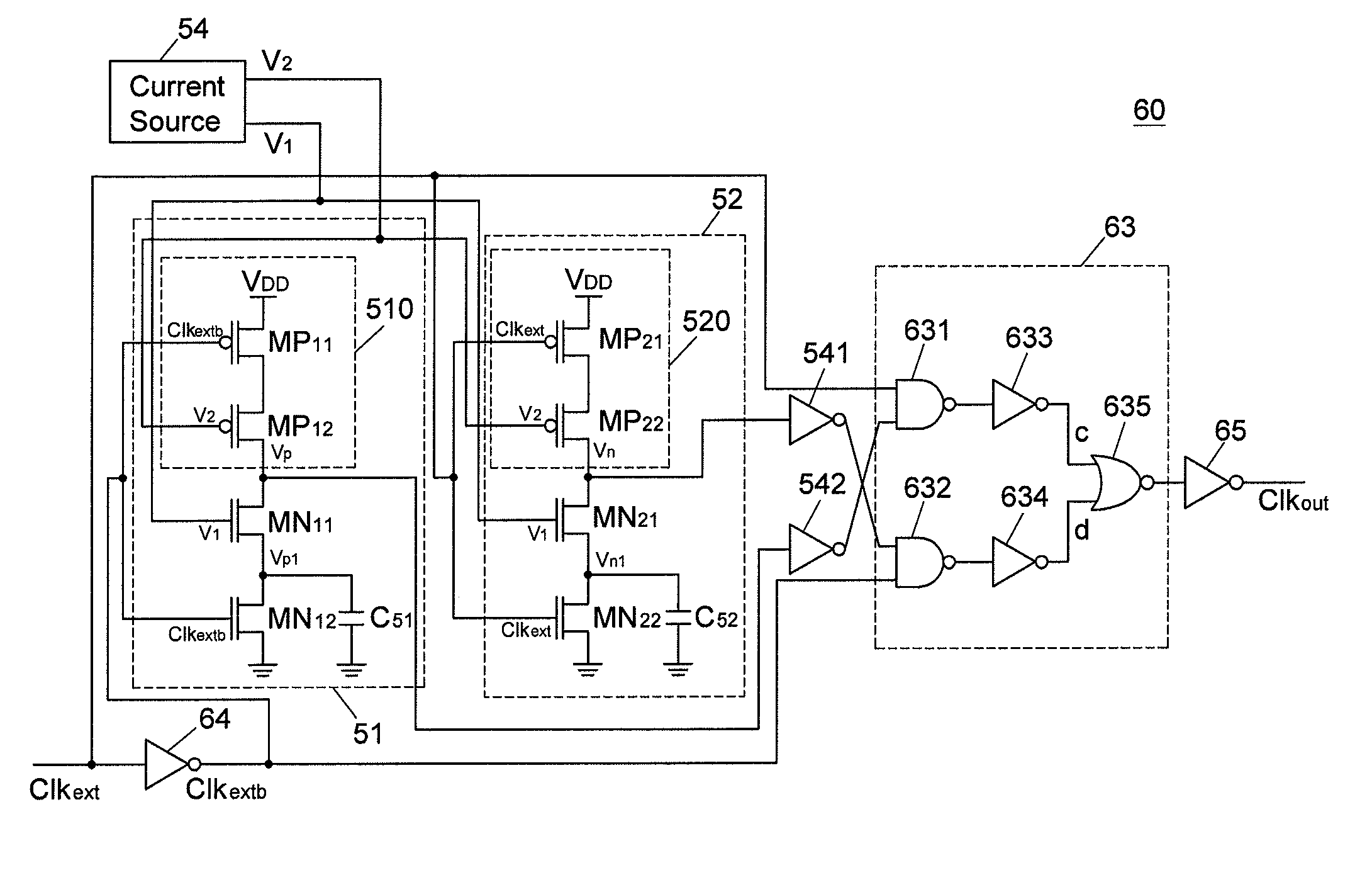
[0025]Reference will now be made in detail to the present examples of the invention, examples of which are illustrated in the accompanying drawings. Wherever possible, the same reference numbers will be used throughout the drawings to refer to the same or like parts.

[0026]FIG. 4A is a circuit diagram of a current source 40 according to an example of the present invention. Referring to FIG. 4A, the current source 40 may include a current mirror 42, a first buffer 40-1 and a second buffer 40-2. The current mirror 42 may include n-type metal-oxide-semiconductor (NMOS) field effect transistors 401 and 402 and p-type metal-oxide-semiconductor (PMOS) field effect transistors 403 and 404. In the current mirror 42, a reference current IREF flowing through the transistors 403 and 401 may “mirror” a current IPTAT flowing through the transistors 404 and 402. The current IPTAT may vary in a way “proportional to absolute temperature” (PTAT). That is, the current IPTAT may vary directly or positi...


PUM


Abstract

The present invention relates to a circuit for generating a clock signal. The circuit comprises a current source to generate a reference current and provide a first voltage V1, a first current generator to generate a first mirror current during a first half cycle based on the reference current, a first capacitor including a first end, and a first transistor having a first threshold voltage VTH1. The first transistor includes a gate to receive the first voltage V1, a drain coupled to the first current generator and a source coupled to the first end of the first capacitor so as to allow the first mirror current to charge the first capacitor during the first half cycle, wherein the period of the first half cycle is a function of the first bias voltage V1 minus the first threshold voltage VTH1.

Description

BACKGROUND OF THE INVENTION[0001]The present invention generally relates to clock generator circuits. More particularly, the present invention relates to clock generator circuits for providing stable clock signals and double frequency clock signals in memory devices. The clock generator circuits in accordance with the present invention may serve as an oscillator or a frequency doubler.[0002]Clock circuits play an important role in modern electronic products. Generally, a clock signal generated by a clock circuit within an integrated circuit or on a printed circuit board of an electronic device is used for signal synchronization in the electronic device. Moreover, a clock circuit may generate clock signals at different clock rates for applications requiring different operation frequencies. The clock signals of different clock rates may be generated by multiplying or dividing the frequency of a reference clock signal.[0003]A clock signal may be generated by a resistance-capacitance (R...

Claims


Application Information

Patent Timeline
Patent Type & Authority Patents(United States)
IPC IPC(8): H03K19/096H03K5/01
CPCH03K19/096H03K5/1565
Inventor LI, CHIA CHINGHO, HSIN YIHUNG, CHUN HSIUNG
Owner MACRONIX INT CO LTD