Method and charge-up circuit capable of adjusting charge-up current
a charge-up current and charge-up circuit technology, applied in the field of charge-up circuits, can solve problems such as difficulty in achieving further reduction of charge-up current fluctuation
- Summary
- Abstract
- Description
- Claims
- Application Information
AI Technical Summary
Benefits of technology
Problems solved by technology
Method used
Image


Examples
first embodiment
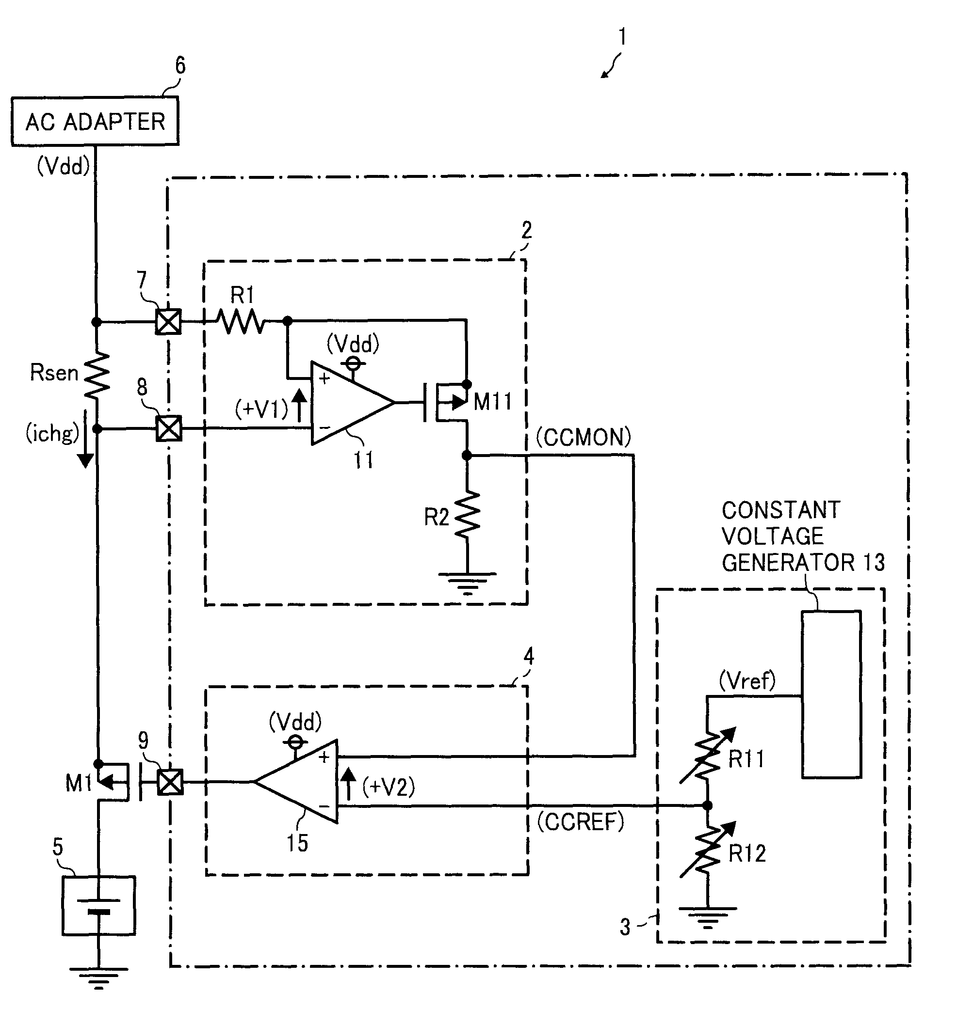
[0018]FIG. 3 is a circuit diagram of a charge-up circuit according to a first example embodiment. The charge-up circuit 1 charges a secondary battery 5 such as a lithium battery from an AC adapter 6 that is a power source with a predetermined charge-up current ichg.
[0019]In FIG. 3, the charge-up circuit 1 includes a resistor Rsen, a charge-up transistor M1 that is formed of a PMOS transistor, a current-to-voltage conversion circuit 2, a reference voltage generator 3, a charge-up current control circuit 4, and a secondary battery 5. The resistor Rsen is used to detect a charge-up current ichg to the secondary battery 5. The charge-up transistor M1 supplies the charge-up current ichg to the secondary battery 5 in accordance with a control signal input to a gate of the charge-up transistor M1. The current-to-voltage conversion circuit 2 generates and outputs a charge-up-current monitor voltage (hereinafter monitor voltage) CCMON by converting the charge-up current ichg flowing through ...
second embodiment
[0033]In the charge-up circuit 1 according to the first example embodiment, there is a possibility that, if the differential amplifier 11 of the current-to-voltage conversion circuit 2 has an input offset that reduces a potential difference generated between both terminals of the resistor R1, the monitor voltage CCMON may become 0 v even when a current flows through the resistor Rsen.
[0034]FIG. 5 is a circuit diagram of a charge-up circuit according to a second example embodiment. The charge-up circuit according to the second embodiment can adjust an input offset so as to have a large input offset larger than the input offset caused by variation during fabrication.
[0035]In FIG. 5, identical reference characters are assigned to identical or similar circuit members shown in FIG. 3 and descriptions thereof are omitted. Further, the charge-up circuit 1 shown in FIG. 3 is changed to a charge-up circuit 1a. Similarly, the differential amplifier 11 is changed to a differential amplifier 11...
PUM
 Abstract
Description
Claims
Application Information