Method and apparatus for minimizing contamination in semiconductor processing chamber

a technology of semiconductor processing chamber and minimizing contamination, which is applied in the direction of conveying, transportation and packaging, pile separation, etc., can solve problems such as device failur

Active Publication Date: 2012-10-16
ASM IP HLDG BV
View PDF69 Cites 414 Cited by
  • Summary
  • Abstract
  • Description
  • Claims
  • Application Information

AI Technical Summary

Benefits of technology

[0012]In the above embodiments, the workpiece support may engage the baseplate opening when the workpiece support is in the processing position. Engaging may include maintaining a gap between the baseplate and the workpiece support. In other arrangements, engaging may create a seal between the baseplate and the workpiece support.

Problems solved by technology

When manufacturing such semiconductor devices, it is desirable that workpieces do not become contaminated by particulates, which may lead to device failure.

Method used


Image

  • Method and apparatus for minimizing contamination in semiconductor processing chamber
  • Method and apparatus for minimizing contamination in semiconductor processing chamber
  • Method and apparatus for minimizing contamination in semiconductor processing chamber

Examples


Embodiment Construction

[0027]Although certain embodiments and examples are disclosed below, it will be understood by those having ordinary skill in the art that the invention extends beyond the specifically disclosed embodiments and / or uses of the invention and obvious modifications and equivalents thereof. Thus, it is intended that the scope of the invention herein disclosed should not be limited by the particular disclosed embodiments described below.

In General

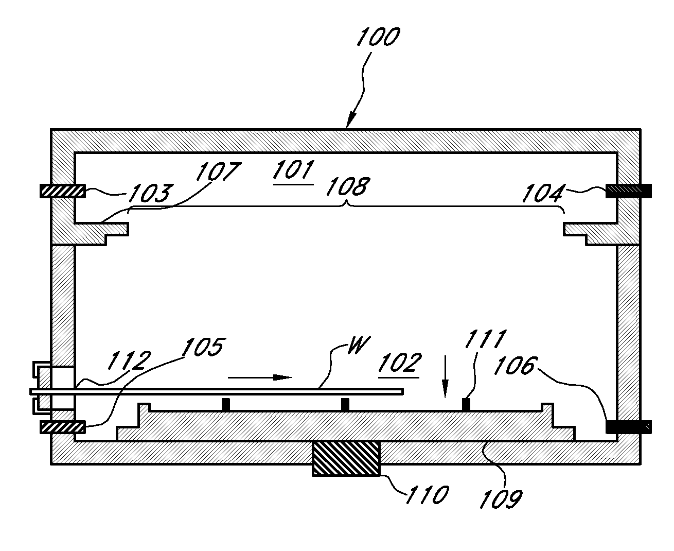
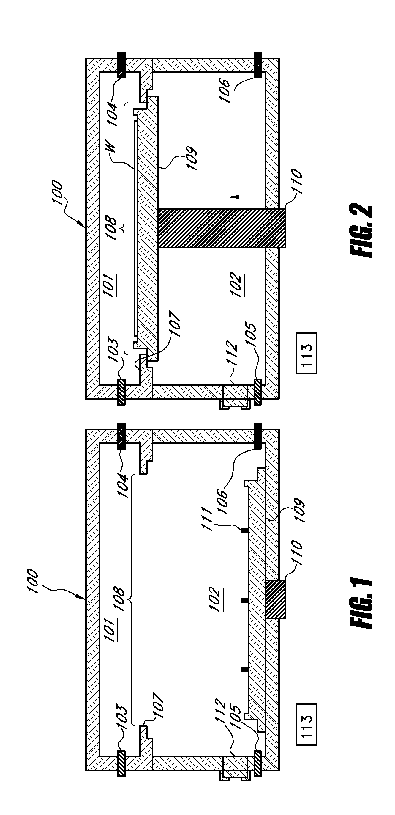
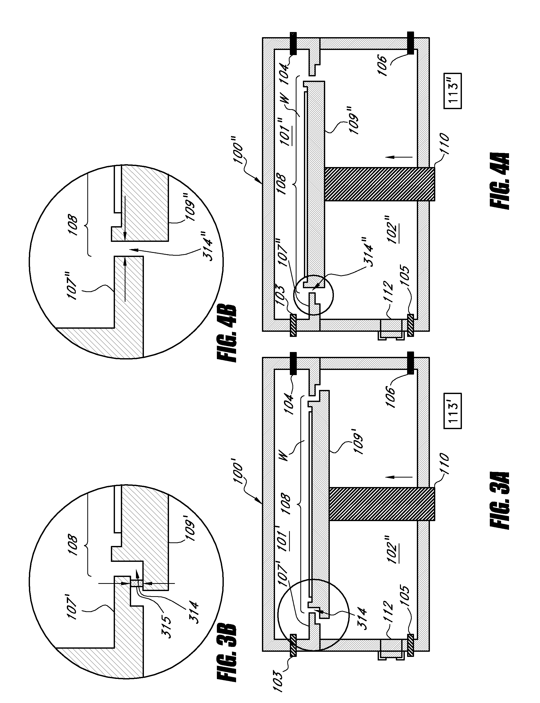
[0028]FIG. 1 schematically illustrates an embodiment of a semiconductor processing apparatus 100 comprising a reaction chamber 101 and a loading chamber 102. Together, the reaction chamber 101 and the loading chamber 102 may be considered a process module. In the illustrated embodiment, the reaction chamber 101 is disposed above the loading chamber 102, and they are separated by a baseplate 107 and a movable pedestal or workpiece support 109, described in more detail below.

[0029]In some embodiments, the reaction chamber 101 may be substantially sm...


PUM

PropertyMeasurementUnit
volumeaaaaaaaaaa
volumeaaaaaaaaaa
volumeaaaaaaaaaa

Abstract

A semiconductor processing apparatus includes a reaction chamber, a loading chamber, a movable support, a drive mechanism, and a control system. The reaction chamber includes a baseplate. The baseplate includes an opening. The movable support is configured to hold a workpiece. The drive mechanism is configured to move a workpiece held on the support towards the opening of the baseplate into a processing position. The control system is configured to create a positive pressure gradient between the reaction chamber and the loading chamber while the workpiece support is in motion. Purge gases flow from the reaction chamber into the loading chamber while the workpiece support is in motion. The control system is configured to create a negative pressure gradient between the reaction chamber and the loading chamber while the workpiece is being processed. Purge gases can flow from the loading chamber into the reaction chamber while the workpiece support is in the processing position, unless the reaction chamber is sealed from the loading chamber in the processing position.

Description

BACKGROUND OF THE INVENTION[0001]1. Field of the Invention[0002]The present invention relates to systems and methods for handling substrates for semiconductor processing.[0003]2. Description of the Related Art[0004]In the processing of semiconductor devices, such as transistors, diodes, and integrated circuits, a plurality of such devices are typically fabricated simultaneously on a thin slice of semiconductor material, termed a substrate, wafer, or workpiece. When manufacturing such semiconductor devices, it is desirable that workpieces do not become contaminated by particulates, which may lead to device failure. Accordingly, reactors in which workpieces are processed are isolated from the exterior of the reaction space to prevent contamination from entering the reaction space.BRIEF SUMMARY OF THE INVENTION[0005]According to one embodiment, a semiconductor processing apparatus includes a cross-flow reaction chamber located above a loading chamber, separated by a baseplate that has ...

Claims


Application Information

Patent Timeline
Patent Type & Authority Patents(United States)
IPC IPC(8): C23C16/00B05C11/00B65H1/00
CPCH01L21/68764H01L21/68742
Inventor REED, JOSEPH CSHERO, ERIC J
Owner ASM IP HLDG BV
Why Eureka
Try Eureka