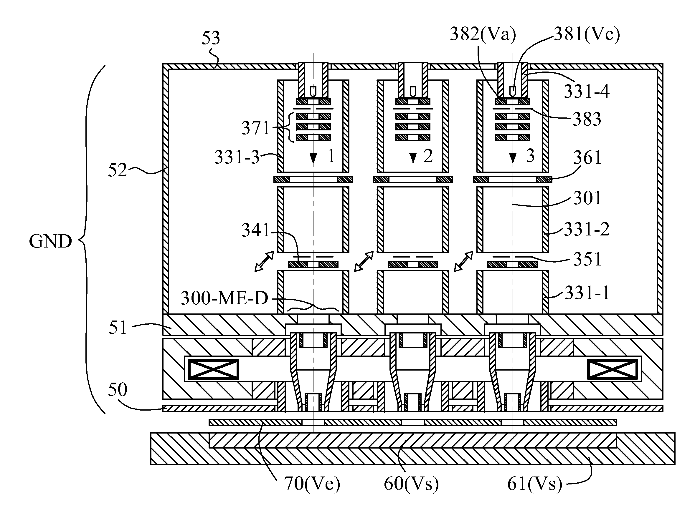
[0011]The object of this invention is to provide an apparatus employing a multi-axis magnetic lens and LVSEM (low-voltage scanning electron microscope) technology, which uses a plurality of low-energy charged particle beams to inspect a specimen in parallel. In this apparatus, by specifically constructing a multi-axis magnetic immersion objective lens required a low coil excitation and overlapping it with an electron deceleration, a multi-axis electromagnetic compound objective is formed to generate lower aberrations and lower radiation damage on specimen. Hence, this invention can provide a higher spatial resolution and a higher throughput than the previous prior arts mentioned above, which can especially benefit the wafer or mask defect inspection in semiconductor yield management. The descriptions below will focus on using a plurality of electron beams, and, however, it would be recognized that the invention has a much broader range of applicability.
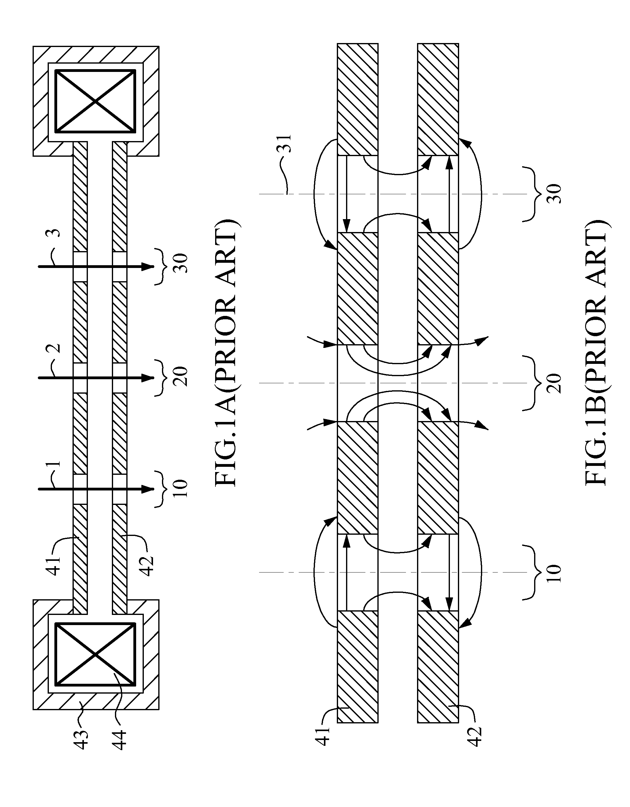
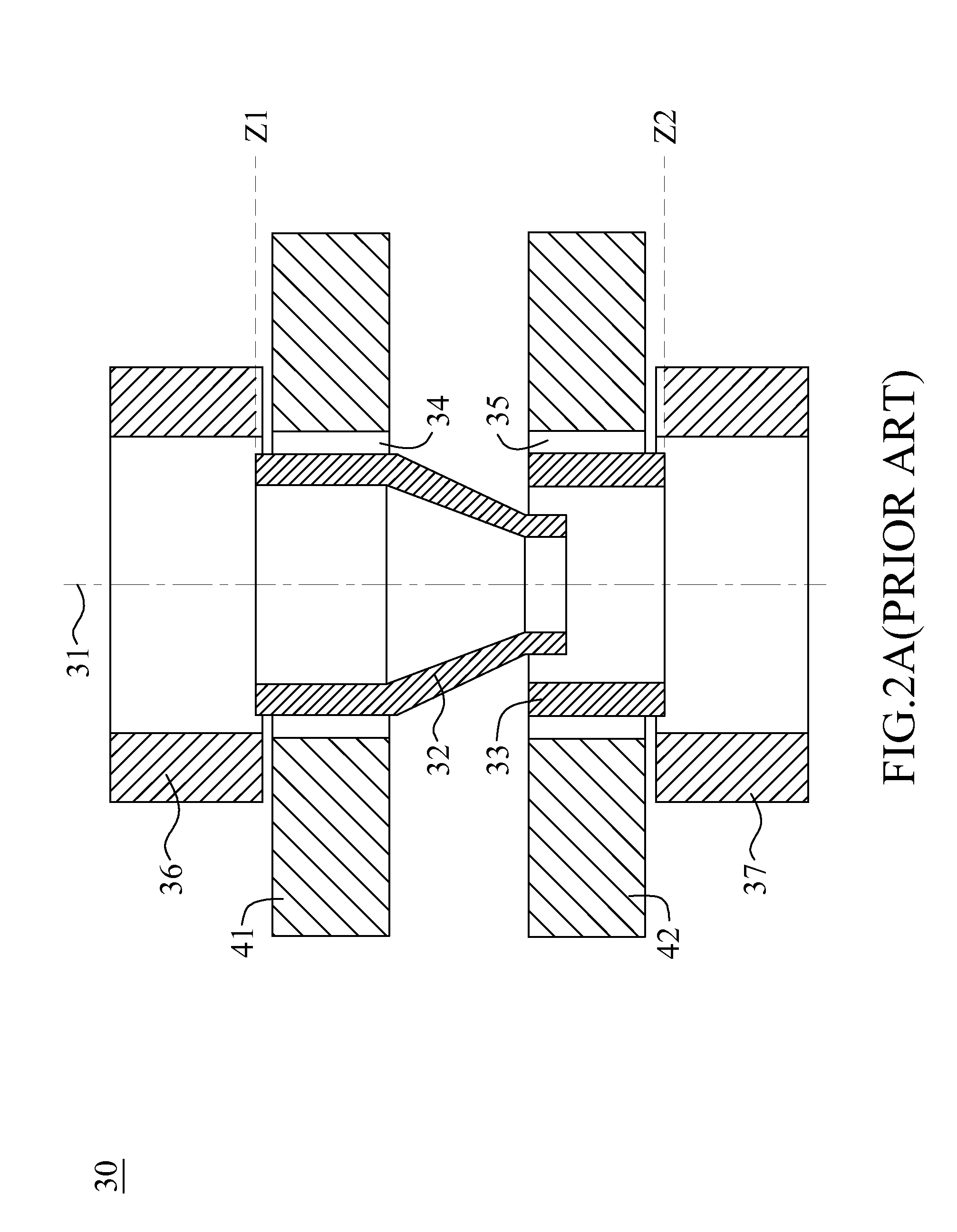
[0012]Accordingly, a first embodiment of a multi-axis magnetic immersion objective lens is provided, which comprises a plurality of magnetic sub-lenses and a magnetic stage for mounting the specimen. Different from prior embodiment of the Chen et al. reference shown in FIG. 2C, a magnetic shielding plate with a plurality of circular openings is inserted between the upper magnetic plate (41) and the magnetic shielding tubes (16, 26, 36) above the upper magnetic plate (41), and called as upper magnetic shielding plate. Secondly, the upper and lower pole-pieces in each magnetic sub-lens are shaped to form a radial magnetic circuit gap. To match this formation, the upper and lower pole-pieces are respectively renamed as inner and outer pole-pieces in this invention. Through the radial magnetic circuit gap in each magnetic sub-lens, a stronger immersion magnetic field is provided on the specimen surface, which can focus an electron beam with lower aberrations. The magnetic specimen stage enhances the magnetic field of each sub-lens and moves its peak closer to the specimen. The first function of this design reduces the common coil excitation required to focus each electron beam. Therefore, the heat cooling is not necessary even when using a shorter working distance, which makes it possible to avoid additionally increasing complexity and instability of the system. A shorter working distance can reduce not only the basic aberrations (spherical and chromatic aberrations), but also the additional aberrations due to the residual non-axisymmetric transverse magnetic fields in front of the specimen. The second function of this design increases the magnetic field immersion on the specimen. It is well known that the stronger the immersion, the smaller the aberrations will be.
[0013]Based on the multi-axis magnetic immersion objective lens mentioned above, secondly, a multi-axis electrostatic immersion objective lens is added to generate a retarding field for deceleration of each electron beam. The multi-axis electrostatic immersion objective lens is constructed by all of the inner pole-pieces which are set at ground potential, the specimen which is set at a negative potential Vs, and a flat electrode plate which is set at a potential Ve equal to or higher than Vs. The flat electrode plate is located in the axial gap between the specimen and the inner pole-pieces, and has a plurality of circular orifices or through round holes, wherein each hole is aligned with an inner pole-piece. The multi-axis electrostatic immersion objective lens actually includes a plurality of electrostatic sub-lenses, wherein each is formed by the inner pole-piece, the flat electrode and the specimen, and therefore overlaps with a magnetic sub-lens in the multi-axis magnetic immersion objective lens. The retarding field generated by each electrostatic sub-lens can provide an effective way to reduce Coulomb effect and imaging aberrations at the same time. By being decelerated to a desired low landing energy just prior to impinging onto the specimen, the electron beam can pass through the remaining part of the electron optics with a higher energy so as to avoid suffering a strong Coulomb effect. The retarding field includes at least a negative electrostatic lens field. The negative aberrations generated by a negative electrostatic lens (divergent lens) can compensate most of the positive aberrations generated by a magnetic sub-lens. The combination of the multi-axis magnetic immersion objective lens and the multi-axis electrostatic immersion objective lens mentioned above is called as multi-axis electromagnetic compound immersion objective lens, and correspondingly a pair of magnetic sub-lens and electrostatic sub-lens overlapping with each other is called as an electromagnetic compound immersion objective sub-lens.
[0015]Therefore, this invention uses the combination of the multi-axis electromagnetic compound lens and a plurality of deflection scanning and compensation units mentioned above to construct an electron apparatus which uses a plurality of electron beams to inspect a specimen in parallel. An individual electron gun is located on the top of each electromagnetic compound immersion objective sub-lens, which generates an individual electron beam. An individual electrostatic condenser is located under each electron gun to focus the electron beam coming from the electron gun. An individual aperture is located under each condenser to limit the current of the electron beam coming from the condenser. A detector with a through round hole is located under each beam limit aperture. The electron beam passing through the hole of the detector then enters the following deflection scanning and compensation unit and electromagnetic compound immersion objective sub-lens. The electromagnetic compound immersion objective sub-lens focuses and decelerates the electron beam to be a low-voltage probe spot on the specimen surface, and the deflection scanning unit of the deflection scanning and compensation unit scans it. Secondary electrons are emitted from the incident site of the probe spot on specimen surface, then pass through the electromagnetic compound immersion objective sub-lens and deflection scanning and compensation unit and finally most of them land on the detector. The space from each electron gun to the top end of each magnetic sub-lens is magnetically shielded by four individual magnetic tubes. Counting from bottom to top, the first tube is stacked on the upper magnetic shielding plate of the multi-axis magnetic immersion objective lens to shield the space from the top end of the magnetic sub-lens to the detector. The second tube is located above the first tube with an axial space gap to shield the space from the beam limit aperture to the vacuum gate valve which separates the gun and the column. The space gap is designed for installing and replacing the detector and beam limit aperture when operating routine maintenance. The third tube is located above the second tube with an axial space gap to shield the space from the gun to the vacuum gate valve. The space gap is designed for installing the vacuum gate valve. The fourth tube is located to overlap with the top end of the third tube from inside, which is especially designed to fully cover the gun tip. A small deviation of an electron trajectory generated by the residual dipole field in the area near the gun tip will be magnified by the following system to a big landing position deviation on the specimen surface. To eliminate the non-axisymmetric transverse magnetic fields in all of the space gaps between the adjacent magnetic tubes, all of the magnetic tubes are covered by a larger common magnetic tube and a larger magnetic shielding plate on the top of the apparatus.

