Wiring board and manufacturing method thereof

a manufacturing method and wiring technology, applied in the direction of resist details, non-metallic protective coating application, synthetic resin layered products, etc., can solve the problems of complex manufacturing steps, electrical short circuit between adjacent connection pads, and inability to perform normal operation of mounted semiconductor integrated circuit elements, etc., to achieve excellent electrical connection reliability

Active Publication Date: 2012-11-06
KYOCERA CORP
View PDF11 Cites 7 Cited by
  • Summary
  • Abstract
  • Description
  • Claims
  • Application Information

AI Technical Summary

Benefits of technology

[0022]One advantage of the invention is to provide a wiring board of high-density wiring having excellent electrical connection reliability as well as a manufacturing method thereof, which enable to properly form solder bumps on individual connection pads for connecting semiconductor elements, without causing any electrical short circuit due to the solder between the adjacent connection pads, thus enabling to surely electrically connect the narrow-pitch electrode terminals of semiconductor integrated circuit elements and the corresponding connection pads.
[0023]The intensive research of the present inventor has led to the present invention based on the following new finding. That is, a solder resist layer is deposited so as to fill up the space between the adjacent connection pads exposed within the slit-shaped openings of the solder resist layer, so that the solder is adhered onto these connection pads. The solder is then melted by heating. At this time, the solder is rejected by the surface of the solder resist layer, thereby enabling solder bumps to be properly formed on the individual connection pads, without causing any electrical short circuit due to the solder between the adjacent connection pads for connecting semiconductor elements. This achieves the wiring board of high-density wiring having excellent electrical connection reliability, which is capable of surely electrically connecting the narrow-pitch electrode terminals of semiconductor integrated circuit elements and the corresponding connection pads.
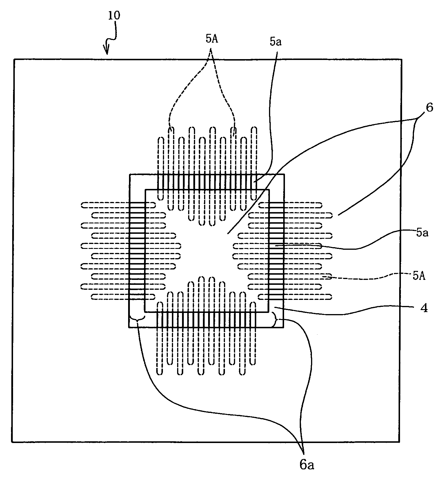
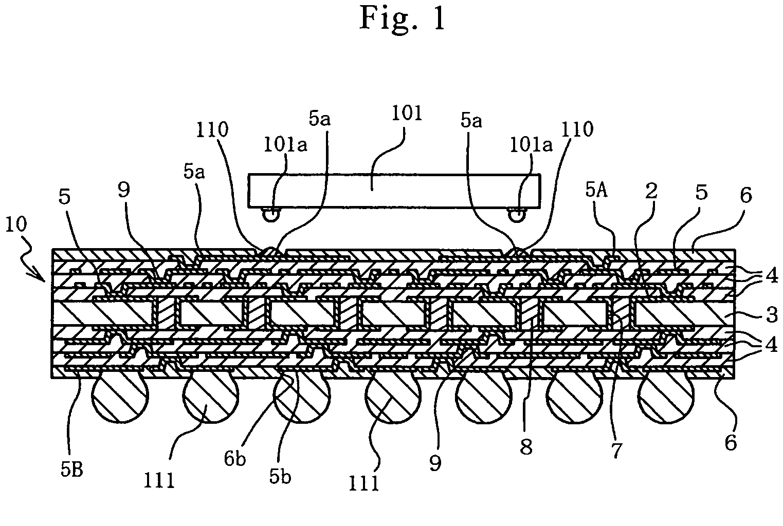
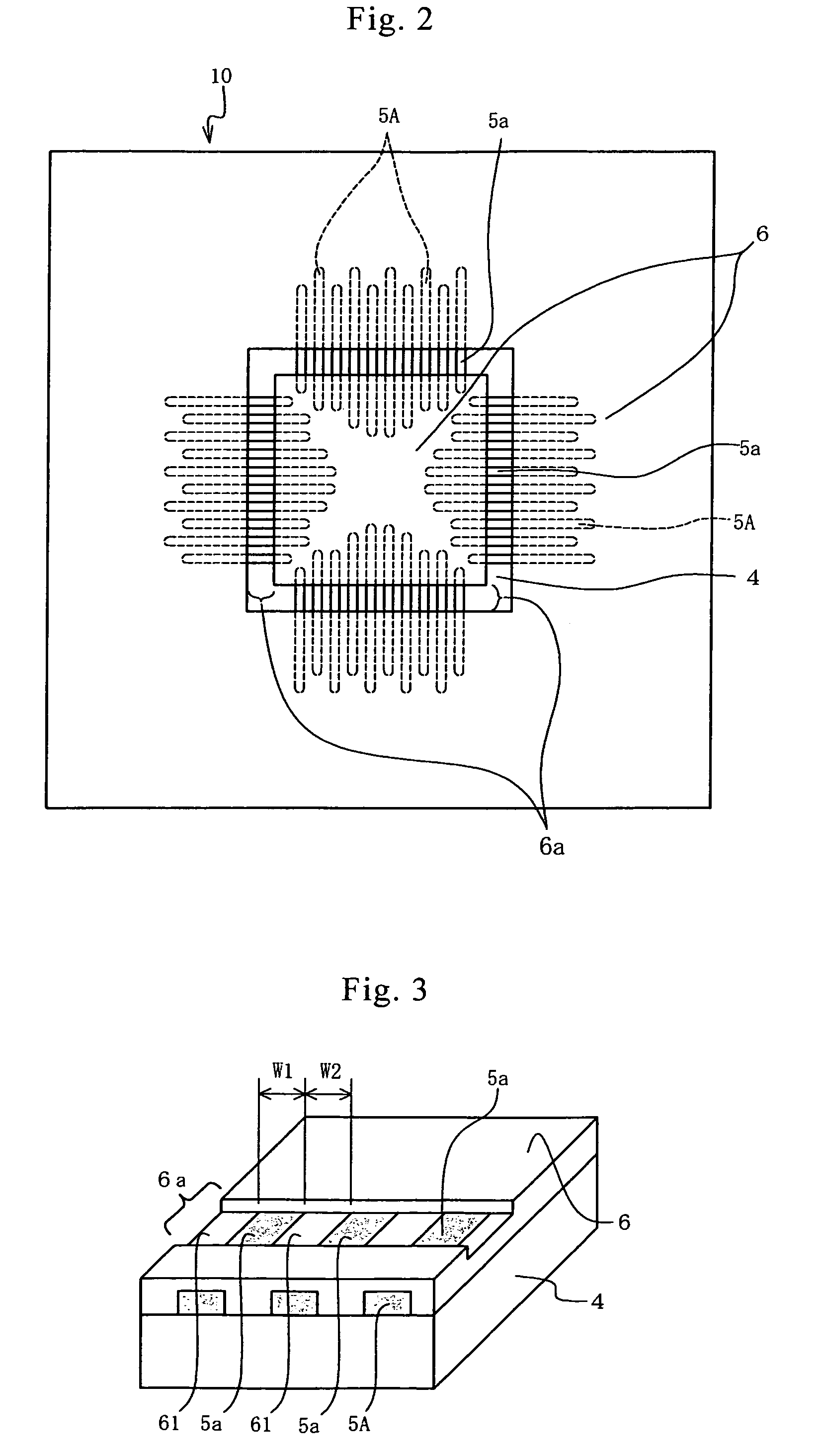
[0024]Specifically, the wiring board of the invention includes alternately laminated insulation layers and wiring conductors, a plurality of strip-shaped wiring conductors for connecting semiconductor elements, arranged side by side on the outermost insulation layer, each wiring conductor partly having a connection pad to which the electrode terminals of the semiconductor elements are connected by flip-chip bonding; and a solder resist layer deposited over the outermost insulation layer and the strip-shaped wiring conductors so as to have slit-shaped openings for exposing the upper surfaces of the connection pads. The solder resist layer fills up the space between the connection pads adjacent to each other and exposed within the slit-shaped openings.
[0025]One method of manufacturing a wiring board of the invention includes the steps of: alternately laminating insulation layers and wiring conductors; arranging side by side, on the outermost insulation layer, a plurality of strip-shaped wiring conductors for connecting semiconductor elements, each wiring conductor partly having a connection pad to which the electrode terminals of the semiconductor elements are connected by flip-chip bonding; depositing a solder resist layer over the entire upper surfaces of the outermost insulation layer and the strip-shaped wiring conductors; and removing the solder resist layer extending over the connection pads and between the adjacent connection pads so that the upper surfaces of the connection pads are exposed and the solder resist layer remains between the connection pads.
[0026]Other method of manufacturing a wiring board of the invention includes the steps of: alternately laminating insulation layers and wiring conductors; arranging side by side, on the outermost insulation layer, a plurality of strip-shaped wiring conductors for connecting semiconductor elements, each wiring conductor partly having a connection pad to which the electrode terminals of the semiconductor elements are connected by flip-chip bonding; depositing a first solder resist layer over the entire upper surfaces of the outermost insulation layer and the strip-shaped wiring conductors; removing the first solder resist layer so that the upper surfaces of the strip-shaped wiring conductors are exposed and the first solder resist layer remains between the adjacent connection pads; and depositing, over the upper surfaces of the first solder resist layer and the strip-shaped wiring boards, a second solder resist layer having slit-shaped openings for exposing the connection pads and the first solder resist layer extending between the adjacent connection pads.
[0027]In accordance with the invention, the solder resist layer is deposited so as to fill up the space between the adjacent connection pads exposed within the slit-shaped openings of the solder resist layer. The wettability on the connection pads is higher than the wettability on the solder resist layer. Therefore, when the solder is adhered onto the connection pads and then melted by heating, even if the melted solder is spread over the space between the adjacent connection pads, the melted solder is rejected by the surface of the solder resist layer, and the solder bumps are formed on the connection pads. This produces the effect of providing the wiring board of high-density wiring having excellent electrical connection reliability which enables to properly form the solder bumps on the individual connection pads for connecting semiconductor elements, without causing any electrical short circuit due to the solder between the adjacent connection pads, thereby ensuring the electrical connection between the narrow-pitch electrode terminals of the semiconductor integrated circuit elements and the corresponding connection pads.

Problems solved by technology

Secondly, the exposed part of the wiring conductors for connecting the semiconductor elements is opposed to the electrode terminals of the semiconductor integrated circuit elements, and then electrically connected to each other through, for example, solder bumps.
This causes an electrical short circuit between the adjacent connection pads 105a, making it impossible to perform the normal operation of the mounted semiconductor integrated circuit elements 101.
For further reduction of the pitch between the connection pads (for example, 50 μm or less), even with the above-mentioned method described in Japanese Patent No. 3420076, the melted solder tends to be connected to the side surfaces of the adjacent connection pads, which may cause an electrical short circuit between the adjacent connection pads.
There remains the problem that the manufacturing steps thereof are complicated and the manufacturing cost thereof is increased.

Method used


Image

  • Wiring board and manufacturing method thereof
  • Wiring board and manufacturing method thereof
  • Wiring board and manufacturing method thereof

Examples


Embodiment Construction

[0042]A first preferred embodiment of the wiring board and the manufacturing method thereof according to the invention will be described in detail with reference to the accompanying drawings. As shown in FIGS. 1 and 2, a wiring board 10 of the present embodiment has a core insulation layer 3 provided with core wiring conductors 2 extending over the upper and lower surfaces of the core insulation layer 3. Buildup insulation layers 4 and buildup wiring conductors 5 are laminated alternately one upon another on the upper and lower surfaces of the core insulation layer 3. Protective solder resist layer 6 is deposited on the outermost surfaces of the laminate.

[0043]The core insulation layer 3 has a thickness of approximately 0.3 to 1.5 mm, and functions as the core material of a wiring board 10. For example, the core insulation layer 3 is composed of an electrically insulation material made by immersing thermosetting resin such as bismaleimide triazine resin or epoxy resin into a glass c...


PUM

PropertyMeasurementUnit
widthaaaaaaaaaa
width W1aaaaaaaaaa
thicknessaaaaaaaaaa

Abstract

In a wiring board, insulation layers and wiring conductors are alternately laminated, and a plurality of strip-shaped wiring conductors for connecting semiconductor elements are arranged side by side on the outermost insulation layer. Each of the wiring conductors partly has a connection pad to which the electrode terminals of the semiconductor elements are connected by flip-chip bonding. In the wiring board, a solder resist layer is deposited over the outermost insulation layer and the strip-shaped wiring conductors so as to have slit-shaped openings for exposing the upper surfaces of the connection pads. The solder resist layer fills up the space between the connection pads adjacent to each other and exposed within the slit-shaped openings.

Description

[0001]Priority is claimed to Japanese Patent Application No. 2007-146108 filed on May 31, 2007, the disclosure of which is incorporated by reference in its entirety.BACKGROUND OF THE INVENTION[0002]1. Field of the Invention[0003]The present invention relates to a wiring board and a manufacturing method thereof. More particularly, the present invention relates to a wiring board and a manufacturing method thereof which are suitable for mounting, for example, peripheral pad type semiconductor integrated circuit elements by flip-chip bonding.[0004]2. Description of Related Art[0005]Examples of semiconductor integrated circuit elements of related art include so-called peripheral pad type semiconductor integrated circuit elements with a large number of electrode terminals arranged along the outer periphery of one major surface thereof. An example of the method of mounting these semiconductor integrated circuit elements on a wiring board is a flip-chip bonding method. In the flip-chip bond...

Claims


Application Information

Patent Timeline
Patent Type & Authority Patents(United States)
IPC IPC(8): H05K1/16
CPCH01L23/49816H01L23/49838H01L2224/0554H01L2224/05568H01L2224/05573H01L2224/16H01L2224/16225H01L2224/32225H01L2224/73204H01L2924/00014H01L2924/01078H01L2924/01079H01L2924/15311H05K3/28H05K3/3452H05K2201/0195H05K2201/09881H05K2201/10674H05K2203/0588H01L2924/00H01L2224/05599H01L2224/0555H01L2224/0556H01L23/48
Inventor OHSUMI, KOHICHI
Owner KYOCERA CORP
Why Eureka
Try Eureka