

Light source device and liquid crystal display apparatus including the same
a liquid crystal display and light source technology, applied in the direction of optics, instruments, optical elements, etc., can solve the problems of adverse effects and adverse effects that may be increased, and achieve the effect of less adverse effects
- Summary
- Abstract
- Description
- Claims
- Application Information
AI Technical Summary
Benefits of technology
Problems solved by technology
Method used
Image

Examples
first embodiment
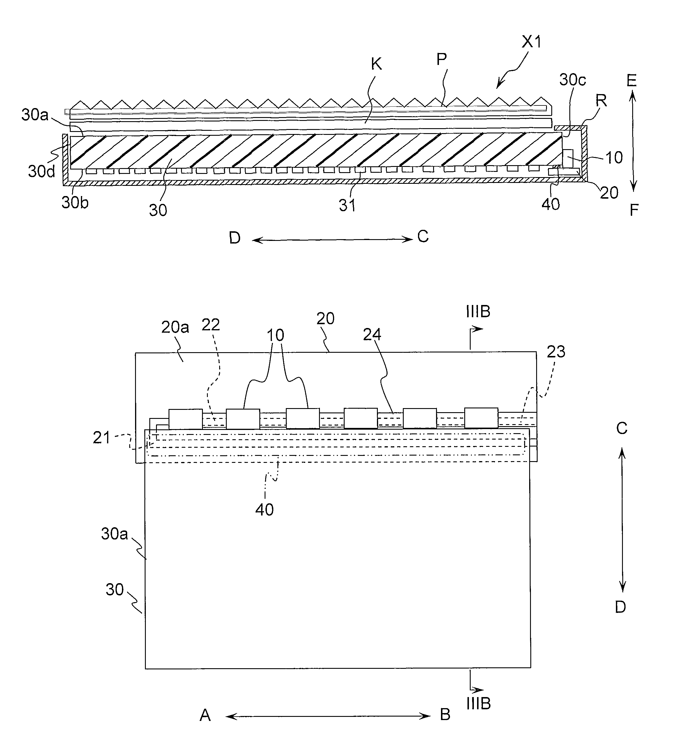
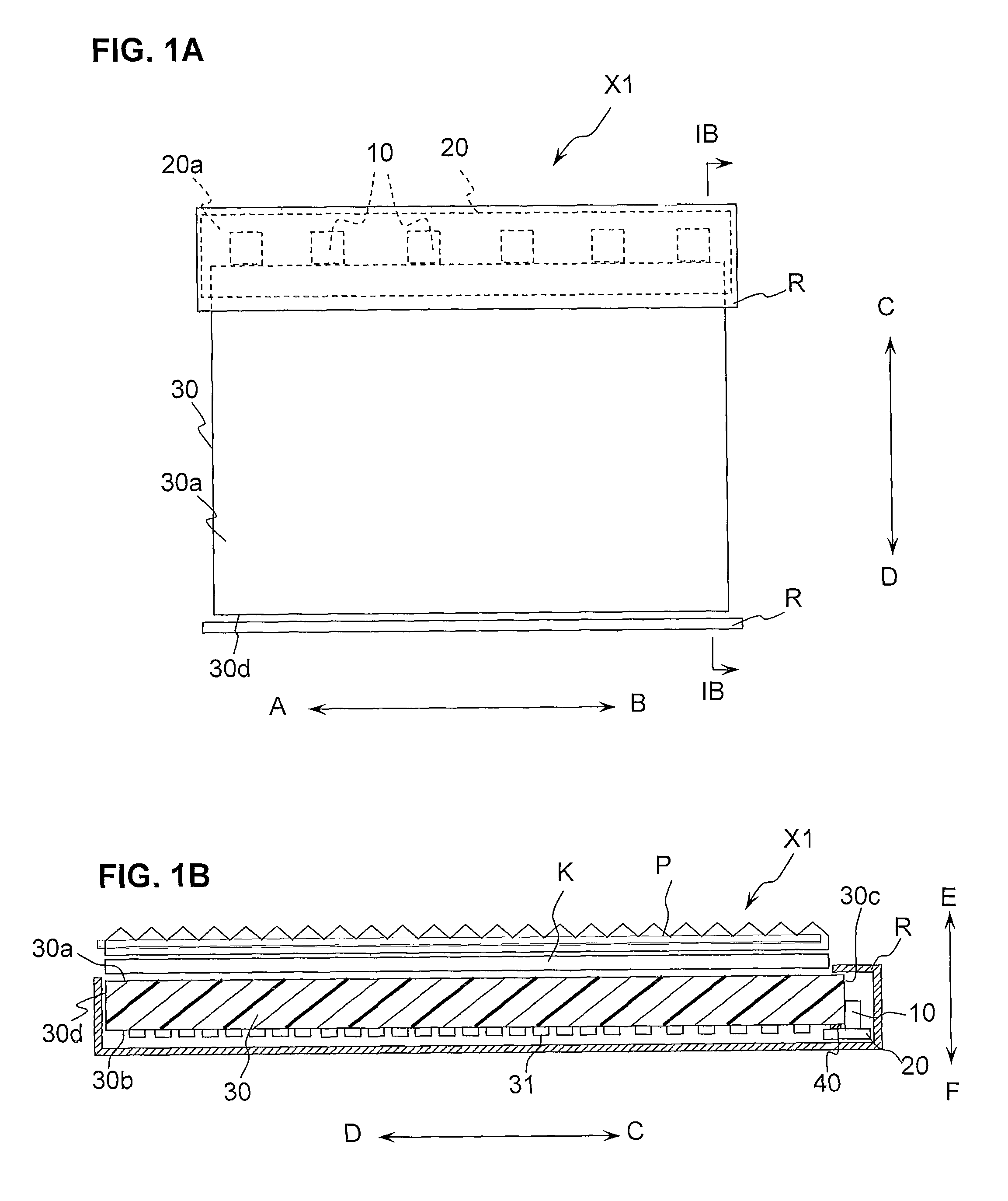
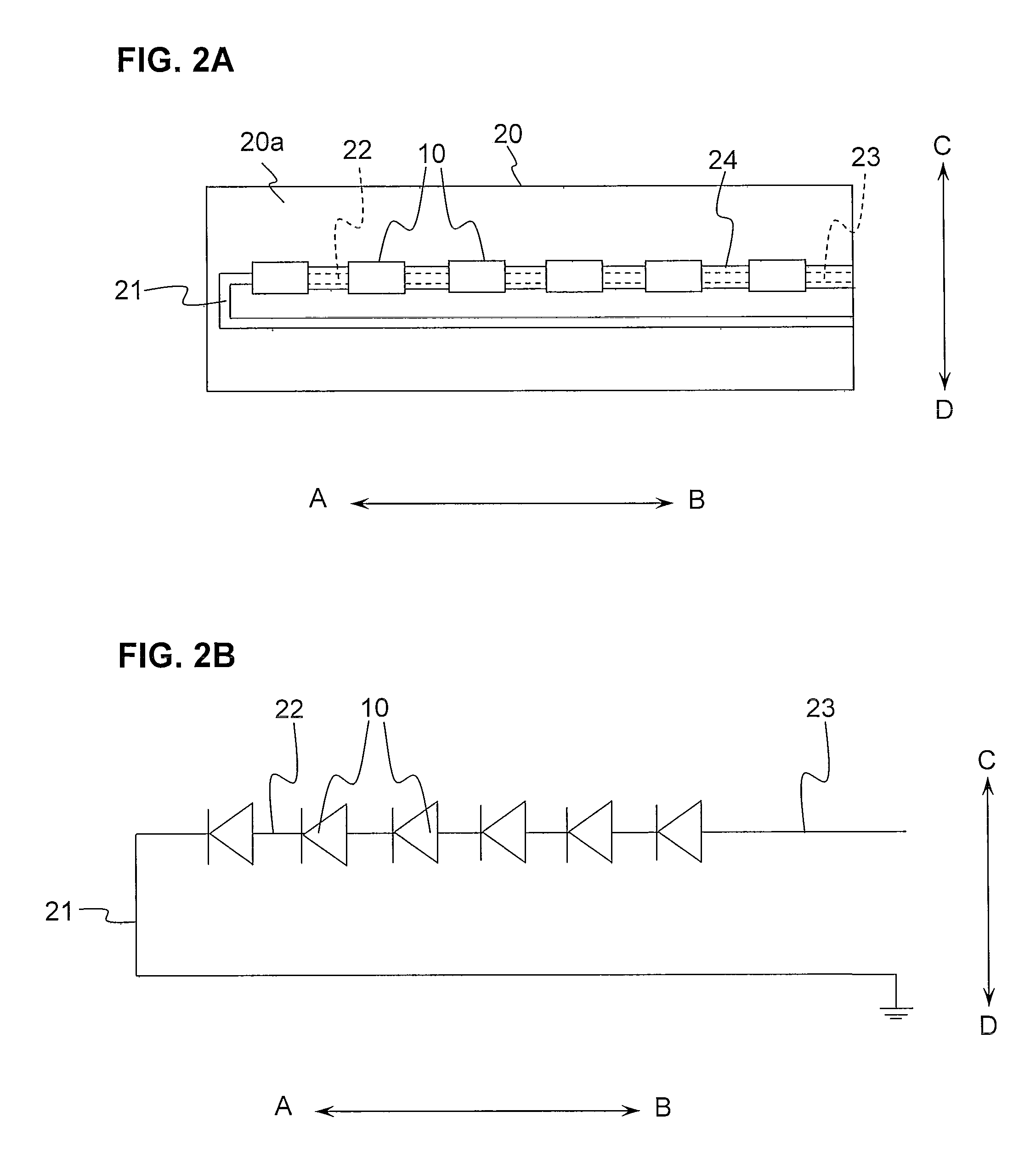
[0021]FIGS. 1A and 1B illustrate a light source device X1. The light source device X1 includes light emitting elements 10, a mounting substrate 20, a light guide substrate 30, a joining member 40 which serves as a conductive intermediate layer, a reflector R, a diffuser K, and a prism P. In the light source device X1, light emitted from the light emitting elements 10 is guided to an object to be irradiated (e.g., a liquid crystal display panel) through the light guide substrate 30. FIG. 2A is a schematic plan view illustrating the light emitting elements 10 and the mounting substrate 20 in the light source device X1. FIG. 2B is an equivalent circuit diagram of the components in FIG. 2A.
[0022]Each light emitting element 10 serves as a member which emits light to the light guide substrate 30. The plurality of (in FIG. 1A, six) light emitting elements 10 are arranged in the direction shown by the arrow AB (hereinafter, referred to as “arrow AB direction”). For the light emitting elemen...
second embodiment
[0039]FIG. 4 is a schematic cross-sectional view of a light source device X2 according to a second embodiment of the present invention. The light source device X2 differs from the light source device X1 in that a mounting substrate 20A is used instead of the mounting substrate 20. FIG. 5A is a schematic plan view illustrating light emitting elements 10 and the mounting substrate 20A in the light source device X2. FIG. 5B is an equivalent circuit diagram of the components in FIG. 5A.
[0040]The mounting substrate 20A serves as a member on which the light emitting elements 10 are mounted. Referring to FIG. 5A, the mounting substrate 20A has a conductive pattern 21A. The mounting substrate 20A has a rectangular parallelepiped shape such that the substrate has an upper surface 20Aa on which the light emitting elements 10 are mounted. The shape of the mounting substrate 20A is not limited to the above one. As a material for the mounting substrate 20A, an insulating resin, such as glass epo...
third embodiment
[0042]FIG. 6A is a schematic cross-sectional view of a light source device X3 according to a third embodiment of the present invention. The light source device X3 differs from the light source device X1 in that a mounting substrate 20B is used instead of the mounting substrate 20 and a light guide substrate 30B is used instead of the light guide substrate 30. FIG. 6B is a schematic plan view illustrating light emitting elements 10 and the mounting substrate 20B in the light source device X3.
[0043]The mounting substrate 20B serves as a member on which the light emitting elements 10 are mounted. Referring to FIG. 6B, the mounting substrate 20B has a conductive pattern 21B. The mounting substrate 20B has a rectangular parallelepiped shape such that the substrate has an upper surface 20Ba on which the light emitting elements 10 are mounted. The shape of the mounting substrate 20B is not limited to the above one. As a material for the mounting substrate 20B, for example, an insulating re...
PUM
| Property | Measurement | Unit |
|---|---|---|
| DA | aaaaa | aaaaa |
| conductive | aaaaa | aaaaa |
| color | aaaaa | aaaaa |
Abstract
Description
Claims
Application Information