Method for modeling devices in a wafer

a technology of modeling devices and wafers, applied in the field of hard disk drives, can solve the problems of ineffective methods, slow speed, and reliance on scanning electron microscopy,

Inactive Publication Date: 2012-11-13
WESTERN DIGITAL TECH INC
View PDF104 Cites 159 Cited by
  • Summary
  • Abstract
  • Description
  • Claims
  • Application Information

AI Technical Summary

Benefits of technology

[0013]Various embodiments of the present invention solve the foregoing problems by providing a non-destructive wafer-level resistance modeling technique that correlates the resistance and inverse stripe height of a device, such as an ELG or even a read head, to be modeled based on measurements taken from an intact wafer. The approach involves a uniquely designed wafer in which otherwise similar devices in different regions have different initial stripe heights, whereby multiple data points correlating measured resistance and stripe height can be determined.

Problems solved by technology

While lapping times, lapping pressures, and other lapping parameters could be standardized for particular types of slider bars 52, such a method can be ineffective due to fabrication variations such as in the deposition of materials of the read / write heads 60, or the wafer cut locations relative to the read / write heads.
This approach, however, relying as it does upon scanning electron microscopy, is complicated and slow, and can only be accomplished after a wafer has been cut into slider bars, and after the slider bars have been at least partially lapped.

Method used


Image

  • Method for modeling devices in a wafer
  • Method for modeling devices in a wafer
  • Method for modeling devices in a wafer

Examples


Embodiment Construction

[0027]In the following detailed description, numerous specific details are set forth to provide a full understanding of the present invention. It will be apparent, however, to one ordinarily skilled in the art that the present invention may be practiced without some of these specific details. In other instances, well-known structures and techniques have not been shown in detail to avoid unnecessarily obscuring the present invention.

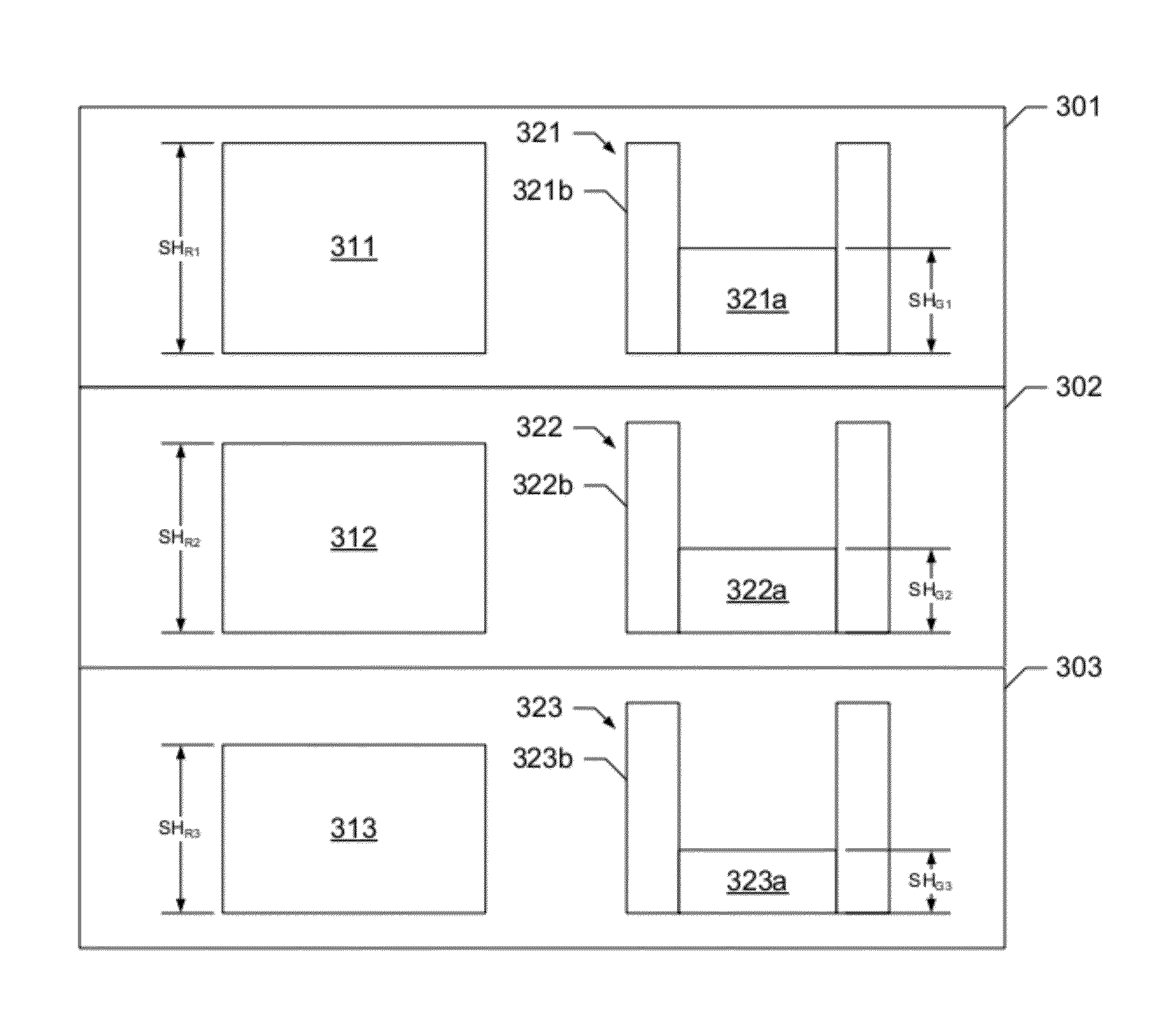
[0028]FIG. 2 illustrates a wafer in accordance with one aspect of the subject disclosure, in which different regions of the wafer include devices with different stripe heights. In this regard, region 201 includes a plurality of ELGs 211, 212 and 213 with a first resistive element stripe height, while region 202 includes a plurality of ELGs with a second resistive element stripe height, and region 203 includes a plurality of ELGs with a third resistive element stripe height. Region 201 further includes a plurality of read heads 221, 222 and 223 with a firs...


PUM

PropertyMeasurementUnit
heightsaaaaaaaaaa
heightsaaaaaaaaaa
track widthaaaaaaaaaa

Abstract

A method for modeling devices in a wafer comprises the step of providing the wafer comprising a first plurality of devices having a track width and a first stripe height, a second plurality of devices having the track width and a second stripe height, and a third plurality of devices having the track width and a third stripe height. The method further comprises the steps of measuring resistance values for the first, second and third plurality of devices to obtain a data set correlating a stripe height and a resistance value for each of the first, second and third plurality of devices, and estimating a linear relationship between resistance and inverse stripe height for the first, second and third plurality of devices based on the data set.

Description

FIELD OF THE INVENTION[0001]The present invention generally relates to hard disk drives and, in particular, relates to the characterization of resistance vs. stripe height from wafer level test data.BACKGROUND OF THE INVENTION[0002]Magnetic disk drives are used to store and retrieve data for digital electronic apparatuses such as computers. In FIGS. 1A and 1B, a magnetic disk drive 10 of the prior art includes a sealed enclosure 12, a disk drive motor 14, a magnetic disk 16, supported for rotation by a spindle S1 of motor 14, an actuator 18 and an arm 20 attached to a spindle S2 of actuator 18. A suspension 22 is coupled at one end to the arm 20, and at its other end to a read / write head or transducer 24. The transducer 24 typically includes an inductive write element with a magnetoresistive read element (shown in FIG. 1C). As the motor 14 rotates the magnetic disk 16, as indicated by the arrow R, an air bearing is formed under the transducer 24 causing it to lift slightly off of th...

Claims


Application Information

Patent Timeline
Patent Type & Authority Patents(United States)
IPC IPC(8): G11B5/127H04R31/00
CPCG11B5/3166G11B5/3169G11B5/3173Y10T29/49036Y10T29/49041Y10T29/49037
Inventor RUDY, STEVEN C.MCKIE, ERIC R.MORAVEC, MARK D.
Owner WESTERN DIGITAL TECH INC
Why Eureka
Try Eureka