Memristors with an electrode metal reservoir for dopants

a technology of metal reservoir and electrode, which is applied in the direction of digital storage, diodes, instruments, etc., can solve the problems of affecting endurance, and prone to loss of switching material

Active Publication Date: 2012-12-04
HEWLETT-PACKARD ENTERPRISE DEV LP
View PDF14 Cites 13 Cited by
  • Summary
  • Abstract
  • Description
  • Claims
  • Application Information

AI Technical Summary

Problems solved by technology

In such memristors, the switching material tends to lose its dopant material.
The loss of dopant material adversely affects the endurance (life of cycling).

Method used


Image

  • Memristors with an electrode metal reservoir for dopants
  • Memristors with an electrode metal reservoir for dopants
  • Memristors with an electrode metal reservoir for dopants

Examples


Embodiment Construction

[0014]Reference is made now in detail to specific examples, which illustrates the best mode presently contemplated by the inventors for practicing the invention. Alternative examples are also briefly described as applicable.

[0015]It is noted that, as used in this specification and the appended claims, the singular forms “a,”“an,” and “the” include plural referents unless the context clearly dictates otherwise.

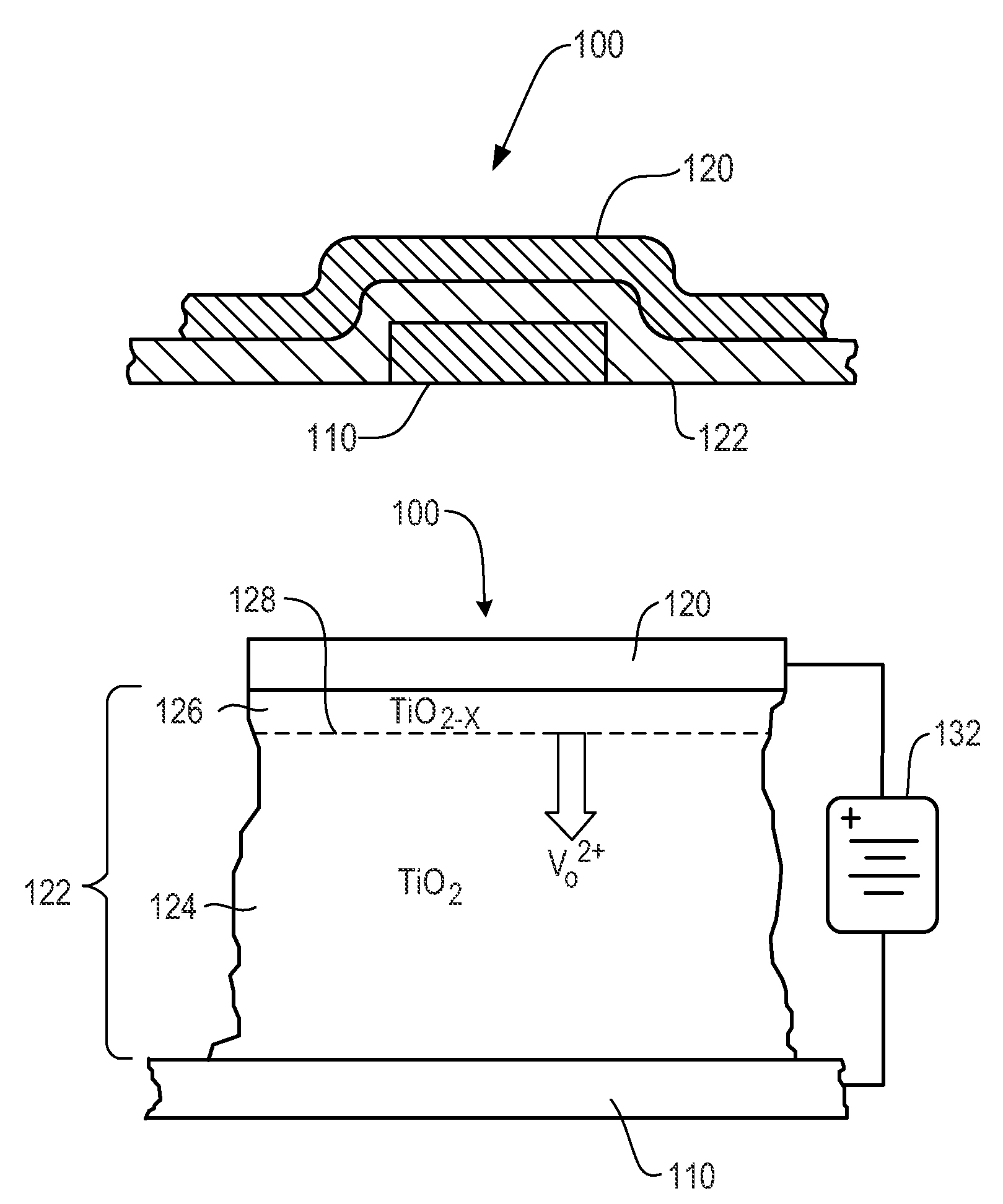
[0016]FIG. 1A shows an example of a nanoscale switching device 100 in accordance with the invention. The switching device 100 includes a bottom, or first, electrode 110 and a top, or second, electrode 120, and an active region 122 disposed between the two electrodes. Each of the bottom and top electrodes 110 and 120 is formed of a conducting material and has a width and a thickness on the nanoscale. As used hereinafter, the term “nanoscale” means the object has one or more dimensions smaller than one micrometer. In this regard, each of the electrodes may be in the form of a nan...


PUM


Abstract

A memristor includes a first electrode of a nanoscale width; a second electrode of a nanoscale width; and an active region disposed between the first and second electrodes. The active region has a both a non-conducting portion and a source of dopants portion induced by electric field. The non-conducting portion comprises an electronically semiconducting or nominally insulating material and a weak ionic conductor switching material capable of carrying a species of dopants and transporting the dopants under an electric field. The non-conducting portion is in contact with the first electrode and the source of dopants portion is in contact with the second electrode. The second electrode comprises a metal reservoir for the dopants. A crossbar array comprising a plurality of the nanoscale switching devices is also provided. A process for making at least one nanoscale switching device is further provided.

Description

STATEMENT REGARDING FEDERALLY SPONSORED RESEARCH OR DEVELOPMENT[0001]This invention has been made with government support. The government has certain rights in the invention.BACKGROUND ART[0002]The continuous trend in the development of electronic devices has been to minimize the sizes of the devices. While the current generation of commercial microelectronics are based on sub-micron design rules, significant research and development efforts are directed towards exploring devices on the nanoscale, with the dimensions of the devices often measured in nanometers or tens of nanometers. Besides the significant reduction of individual device size and much higher packing density compared to microscale devices, nanoscale devices may also provide new functionalities due to physical phenomena on the nanoscale that are not observed on the microscale.[0003]For instance, electronic switching in nanoscale devices using titanium oxide as the switching material has recently been reported. The resi...

Claims


Application Information

Patent Timeline
Patent Type & Authority Patents(United States)
IPC IPC(8): H01L29/8605H01L21/04G11C11/21
CPCH01L45/1233H01L45/146H01L27/2463H01L45/1266H01L45/145H01L45/08H10B63/80H10N70/24H10N70/8416H10N70/883H10N70/826H10N70/8833H10N70/046
Inventor YANG, JIANHUAYI, WEISTUKE, MICHAEL JOSEFWANG, SHIH-YUAN
Owner HEWLETT-PACKARD ENTERPRISE DEV LP
Why Eureka
Try Eureka