Circuit architecture for the parallel supplying during electric or electromagnetic testing of a plurality of electronic devices integrated on a semiconductor wafer

a technology of circuit architecture and electronic devices, applied in electrical testing, electrical apparatus, instruments, etc., can solve problems such as loss of electric performance, damage to the pads of electronic devices selected for testing, and problems in the assembly of electronic devices

Active Publication Date: 2013-02-19
STMICROELECTRONICS SRL
View PDF47 Cites 7 Cited by
  • Summary
  • Abstract
  • Description
  • Claims
  • Application Information

AI Technical Summary

Benefits of technology

[0028]One embodiment is a circuit architecture for the parallel supplying of power during an electric or electromagnetic testing of a plurality of electronic devices each integrated on a same semiconductor wafer wherein said electronic devices are neatly provided on said semiconductor wafer through integration techniques and have edges bounded by separation scribe lines. The circuit architecture comprises:

Problems solved by technology

In fact, although advantageous under several aspects, and substantially meeting the aim, the probes which connect the tester to the wafer have some drawbacks; for example, they can lead to a damaging of the pads of the electronic devices selected for the testing.
This damaging can cause problems in the assembly of the electronic devices that have passed the quality control at the end of the testing.
This implies an increase of the contacting problems, and thus an increase of the electric continuity problems between the probe card and the wafer, or, better, between the probes and the pads of the electronic device, with subsequent problems of loss of electric performance.
Other problems are due to the mechanical limits of last generation state-of-the-art electronic devices, which have a high number of pads to be contacted, or have pads of reduced area, or even pads which are often very close to each other.
This will imply an increase of area of each electronic device, even if this need is to be considered unavoidable.
However, the parallel electric or electromagnetic testing of a plurality of devices arranged on a single wafer, raises the problem of how to supply them enough to operate under testing conditions.
In substance, the problem of supplying the various electronic devices which are tested in parallel is tied to the fact that these devices should operate simultaneously during the testing.

Method used


Image

  • Circuit architecture for the parallel supplying during electric or electromagnetic testing of a plurality of electronic devices integrated on a semiconductor wafer
  • Circuit architecture for the parallel supplying during electric or electromagnetic testing of a plurality of electronic devices integrated on a semiconductor wafer
  • Circuit architecture for the parallel supplying during electric or electromagnetic testing of a plurality of electronic devices integrated on a semiconductor wafer

Examples


Embodiment Construction

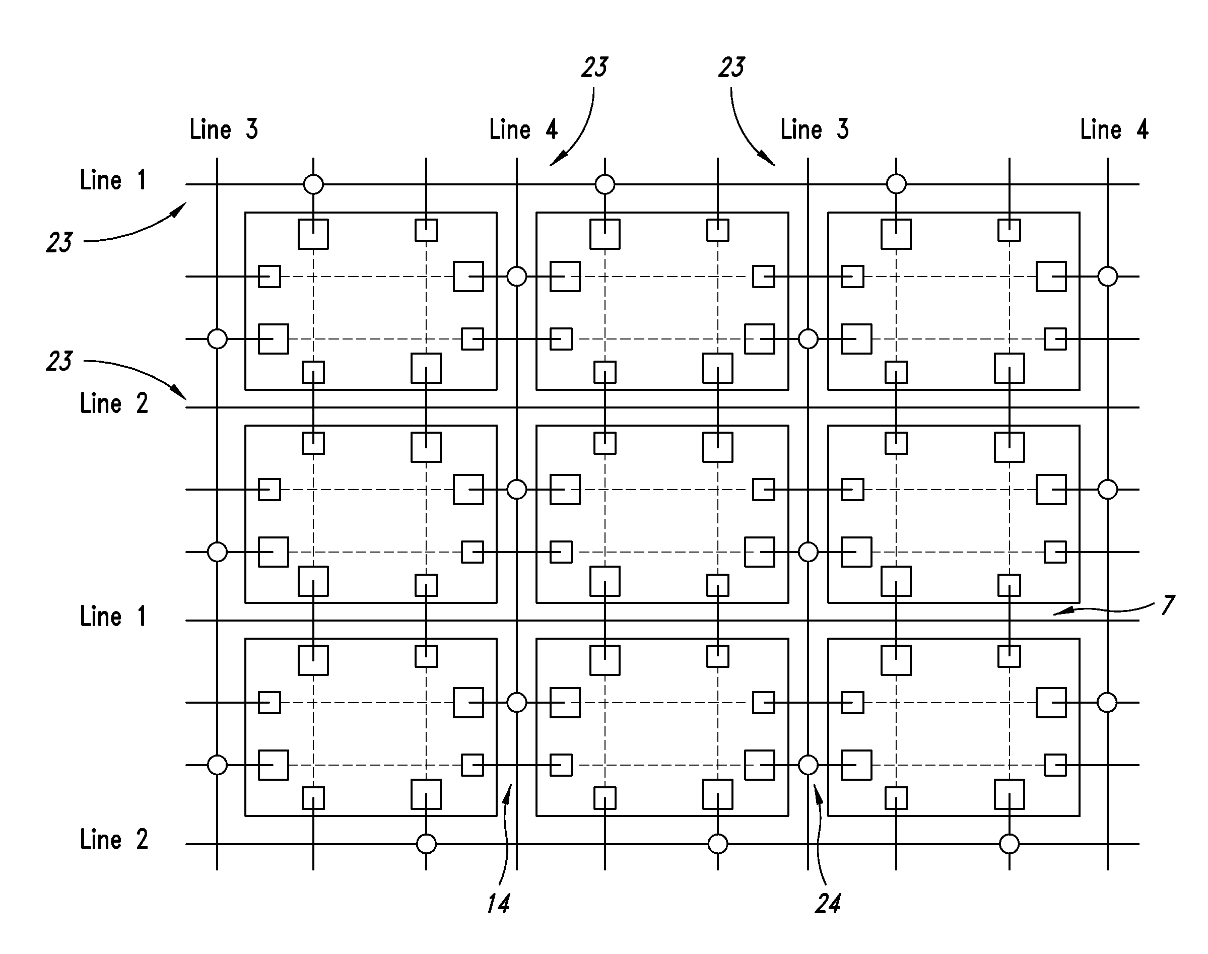
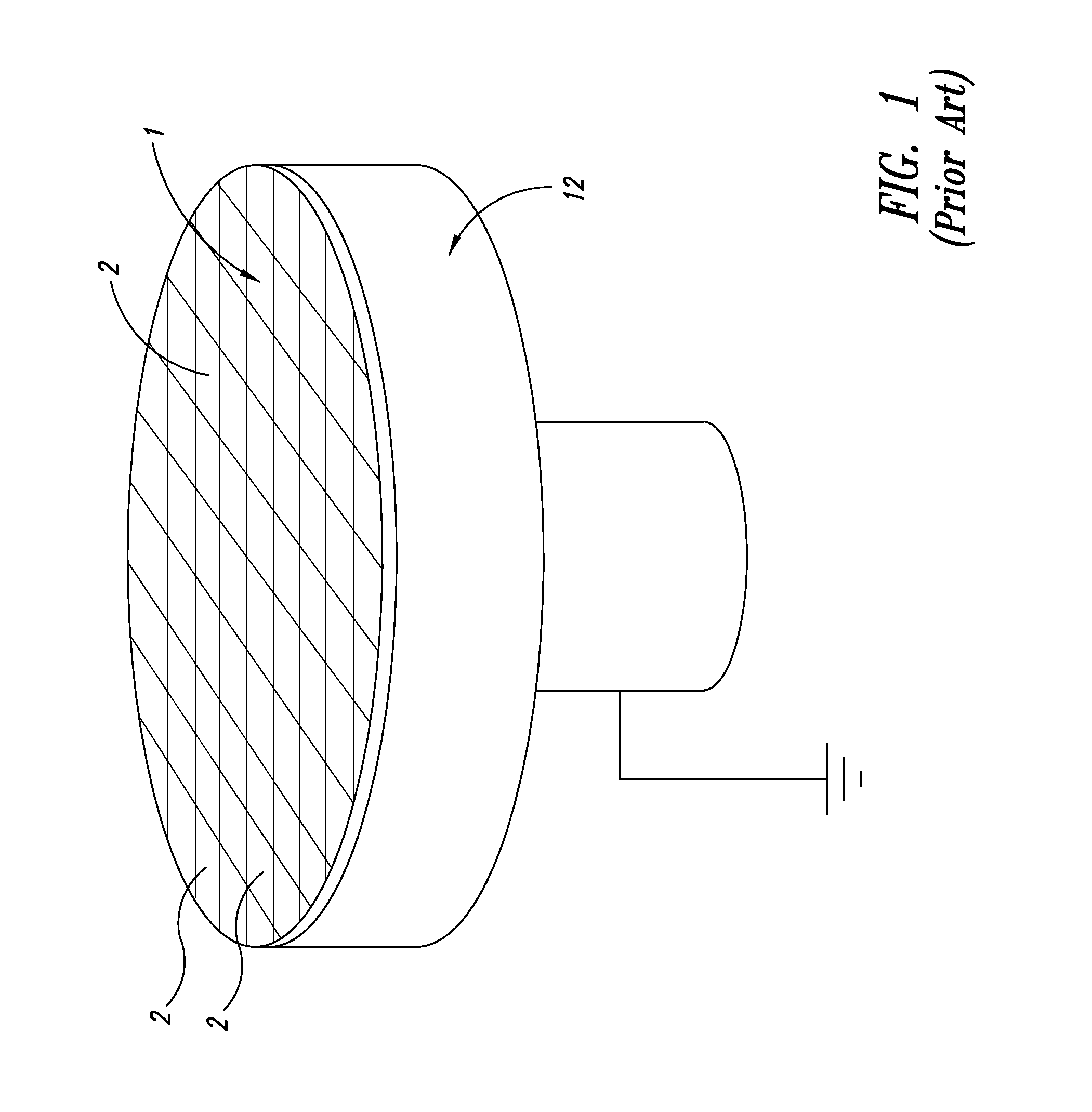
[0084]With reference to these figures, and in particular to the example of FIG. 1, a wafer of semiconductor material is globally and schematically indicated with 1, several semiconductor electronic devices 2 being neatly provided on a surface of the same according to known monolithic integration techniques.

[0085]The wafer 1 is housed on a support 12 which allows electrical connection of the lower or back surface of the wafer, on which the electronic devices 2 are realized, to a reference potential, for example a signal ground or a power supply.

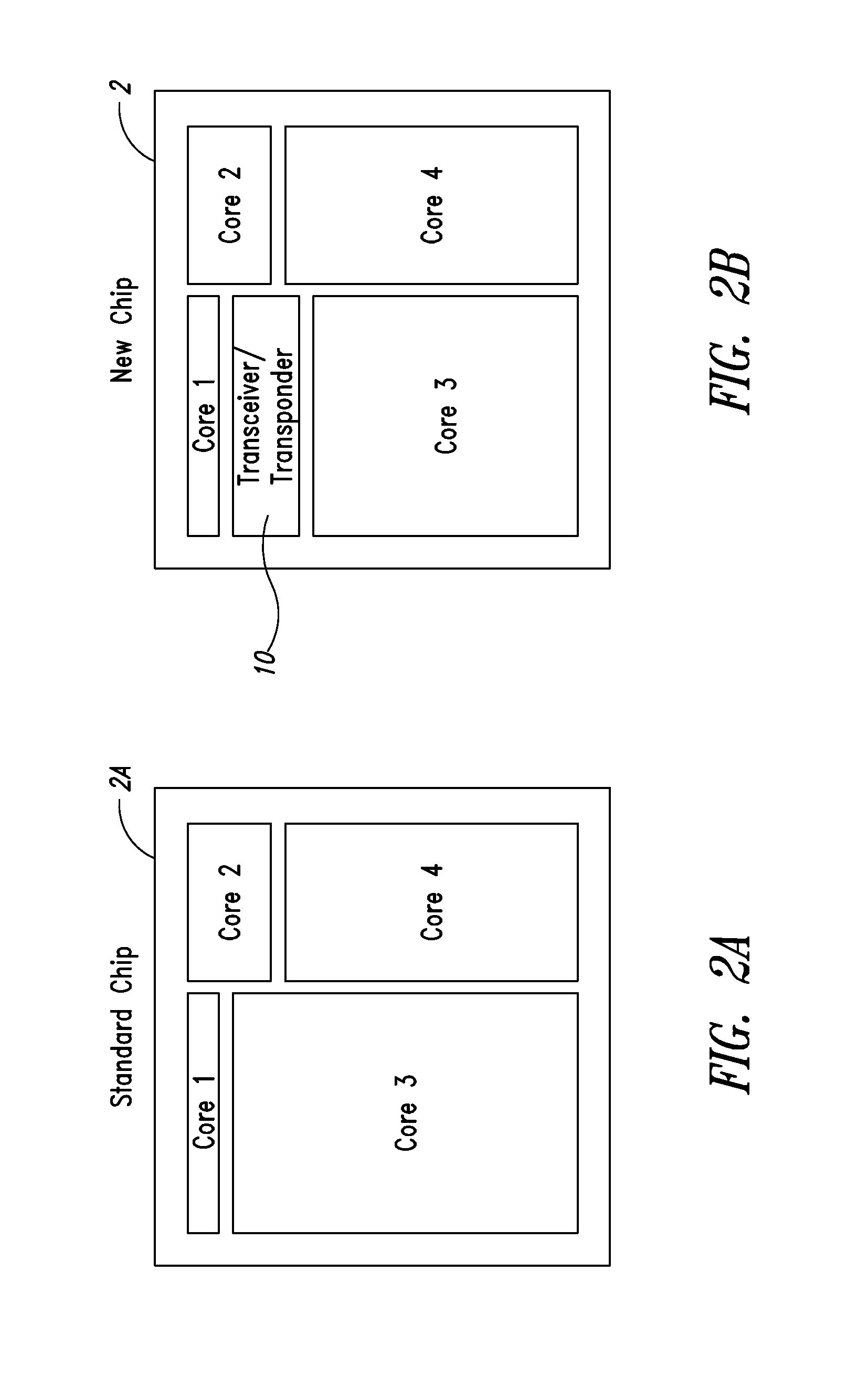
[0086]Most of the structure, nature and operation mode of the electronic devices 2 goes beyond the content of the present disclosure. An electronic device 2 according to one embodiment of the present disclosure is shown in FIG. 2B and is provided with a circuit portion 10 of the transceiver or transponder type which can be used for transmitting electric / electromagnetic signals from and towards the electronic device 2 with or without a direct c...


PUM


Abstract

A circuit architecture provides for the parallel supplying of power during electric or electromagnetic testing of electronic devices integrated on a same semiconductor wafer and bounded by scribe lines. The circuit architecture comprises a conductive grid interconnecting the electronic devices and having a portion external to the devices and a portion internal to the devices. The external portion extends along the scribe lines; and the internal portion extends within at least a part of the devices. The circuit architecture includes interconnection pads between the external portion and the internal portion of the conductive grid and provided on at least a part of the devices, the interconnection pads forming, along with the internal and external portions, power supply lines which are common to different electronic devices of the group.

Description

BACKGROUND[0001]1. Technical Field[0002]The present disclosure relates to a circuit architecture and a method for solving the problem of the parallel supplying during the testing steps, in particular electromagnetic wafer sort (EMWS) testing, of a plurality of electronic devices integrated on a semiconductor wafer and arranged in parallel on said wafer.[0003]The disclosure further relates to creating connections between the various devices on the wafer, for then using them during the testing of the wafer itself to supply them, due to the non-negligible power required by the operation of the devices themselves.[0004]The disclosure particularly, but not exclusively, relates to applications of a process of electric wafer sort (EWS) and / or electromagnetic wafer sort (EMWS) and / or wafer level burn-in (WLBI) intended for the quality control in the manufacturing of electronic devices integrated on semiconductor wafer.[0005]2. Description of the Related Art[0006]As it is well known in this ...

Claims


Application Information

Patent Timeline
Patent Type & Authority Patents(United States)
IPC IPC(8): H01L23/58
CPCH01L22/32G01R31/2884H01L2924/0002H01L2924/00
Inventor PAGANI, ALBERTO
Owner STMICROELECTRONICS SRL
Why Eureka
Try Eureka