
Pixel circuit, a solid-state image sensing device, and a camera system that facilitates charge transfer within a pixel

a solid-state image sensing and pixel technology, applied in the field of pixel circuits, can solve the problems of inability to raise vf or raise the s/n-ratio, limited dynamic range of the potential of the fd node b>7/b>, etc., to facilitate charge transfer within the pixel, improve imaging performance, and increase the amount of accumulated charge and sensitivity

Active Publication Date: 2013-06-04
SONY SEMICON SOLUTIONS CORP
View PDF14 Cites 3 Cited by
  • Summary
  • Abstract
  • Description
  • Claims
  • Application Information

AI Technical Summary

Benefits of technology

[0066]However, for the purpose, it is necessary to provide an excessive device and an excessive signal line in each pixel, and there is a disadvantage that the aperture ratio of the pixel is reduced.
[0067]Thus, it is desirable to provide a pixel circuit, a solid-state image sensing device, and a camera system that can facilitate charge transfer within a pixel, improve amounts of accumulated charge and sensitivity, and improve imaging performance without reducing aperture ratio of the pixel.
[0069]A solid-state image sensing device according to another embodiment of the invention has a pixel unit in which plural pixel circuits are arranged, and a pixel drive unit that drives the pixel circuits of the pixel unit and reads out pixel signals, wherein each pixel circuit includes a photoelectric conversion device, a source-follower circuit, a transfer transistor that transfers charge generated in the photoelectric conversion device to an input node of the source-follower circuit, and a readout system that reads out a signal in response to the generated charge through the source-follower circuit, and wherein the readout system floats the input node of the source-follower circuit and turns on the transfer transistor to transfer the signal charge to the input node, includes a function of turning off the transfer transistor, sensing an output node potential of the source-follower circuit, and reading out an output signal, and further includes an output modulation degree control function unit that temporarily reduces an output modulation degree of the source-follower circuit when the transfer transistor is turned on.
[0071]According to the embodiments of the invention, charge transfer within a pixel can be facilitated, amounts of accumulated charge and sensitivity can be improved, and imaging performance can be improved without reduction of the aperture ratio of the pixel.

Problems solved by technology

However, for the necessity, there are disadvantages that the dynamic range of the potential of the FD node 7 is limited, and it may be impossible to sufficiently raise ΔVf or raise the S / N-ratio.

Method used


Image

  • Pixel circuit, a solid-state image sensing device, and a camera system that facilitates charge transfer within a pixel
  • Pixel circuit, a solid-state image sensing device, and a camera system that facilitates charge transfer within a pixel
  • Pixel circuit, a solid-state image sensing device, and a camera system that facilitates charge transfer within a pixel

Examples


first embodiment

1. First Embodiment

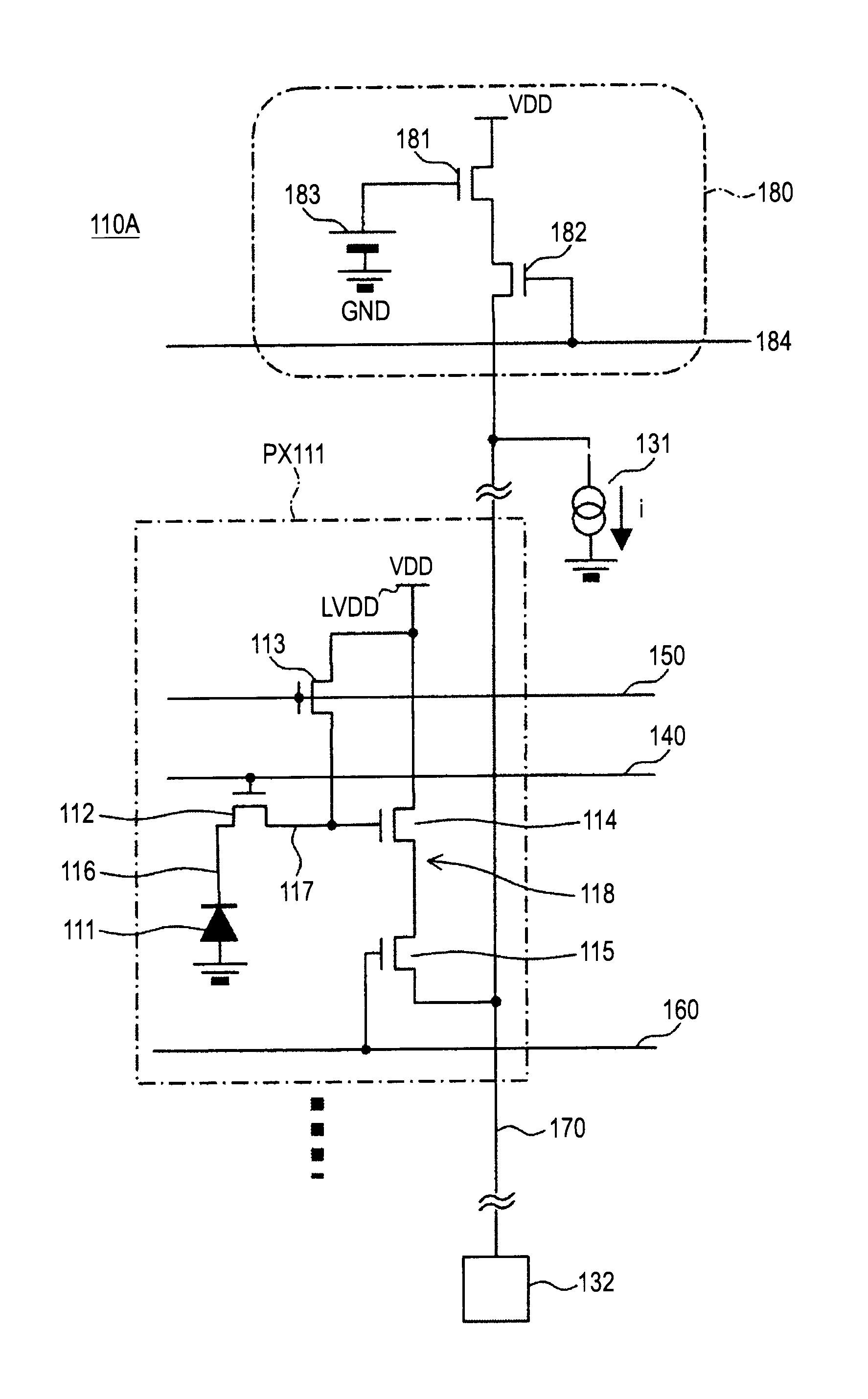
[0109]FIG. 6 shows a pixel circuit of a CMOS image sensor according to the first embodiment of the invention.

[0110]In the pixel circuit 110A in FIG. 6, the configuration unit shown by a dotted line is a unit pixel circuit PX111.

[0111]The unit pixel circuit PX111 has a photodiode 111 as a photoelectric conversion device, a transfer transistor 112, a reset transistor 113, an amp transistor 114, a selection transistor 115, an accumulation node 116, and an FD node 117.

[0112]The amp transistor 114 forms an amp circuit 118, and the FD node 117 forms the input node of the amp circuit 118.

[0113]The transfer transistor 112 of the first embodiment is connected between the photodiode 111 and the FD node 117 as the output node. The gate electrode of the transfer transistor 112 is commonly connected to the transfer line 140.

[0114]The reset transistor 113 is connected between a power supply line LVDD and the FD node 117 and the gate electrode is connected to the reset line 150....

second embodiment

2. Second Embodiment

[0211]FIG. 13 shows a pixel circuit of a CMOS image sensor according to the second embodiment of the invention.

[0212]A pixel circuit 110D according to the second embodiment is different from the pixel circuit 110A according to the first embodiment in the following point.

[0213]That is, in the pixel circuit 110D, to the vertical signal line 170, for example, not the clamp circuit, but a dummy pixel 190 at the reset level is connected.

[0214]According to the second embodiment, a similar effect to that in the above described first embodiment can be obtained.

[0215]In the pixel circuit 110D, to the vertical signal line 170, the source-follower output of the dummy pixel (DM) 190 is temporarily connected in addition to the source-follower output of the selected pixel PX111.

[0216]The dummy pixel (DM) 190 has the same internal configuration as that of the unit pixel PX111 shown in FIG. 6, for example, in which the transfer transistor 112 is constantly off and the reset tran...

third embodiment

3. Third Embodiment

[0219]FIG. 14 shows a pixel circuit of a CMOS image sensor according to the third embodiment of the invention.

[0220]A pixel circuit 110E according to the third embodiment is different from the pixel circuit 110A according to the first embodiment in the following point.

[0221]That is, in the pixel circuit 110E, the source-follower output itself can be fixed to the power supply voltage VDD via a switch device 200.

[0222]In this example, the switch device 200 is formed by a PMOS transistor, and its drain is connected to the vertical signal line 170, the source is connected to the power supply line LVDD, and the gate electrode is connected to a power supply connection line 201.

[0223]The power supply connection line 201 is switched from the high level to the low level over the period in which the selected pixel PX111 performs internal charge transfer for readout.

[0224]Thereby, the switch device 200 as the PMOS transistor is temporarily turned on, and the vertical signal ...


PUM


Abstract

A pixel circuit includes: a photoelectric conversion device; a source-follower circuit; a transfer transistor that transfers charge generated in the photoelectric conversion device to an input node of the source-follower circuit; and a readout system that reads out a signal in response to the generated charge through the source-follower circuit, wherein the readout system floats the input node of the source-follower circuit and turns on the transfer transistor to transfer the signal charge to the input node, includes a function of turning off the transfer transistor, sensing an output node potential of the source-follower circuit, and reading out an output signal, and further includes an output modulation degree control function unit that temporarily reduces an output modulation degree of the source-follower circuit when the transfer transistor is turned on.

Description

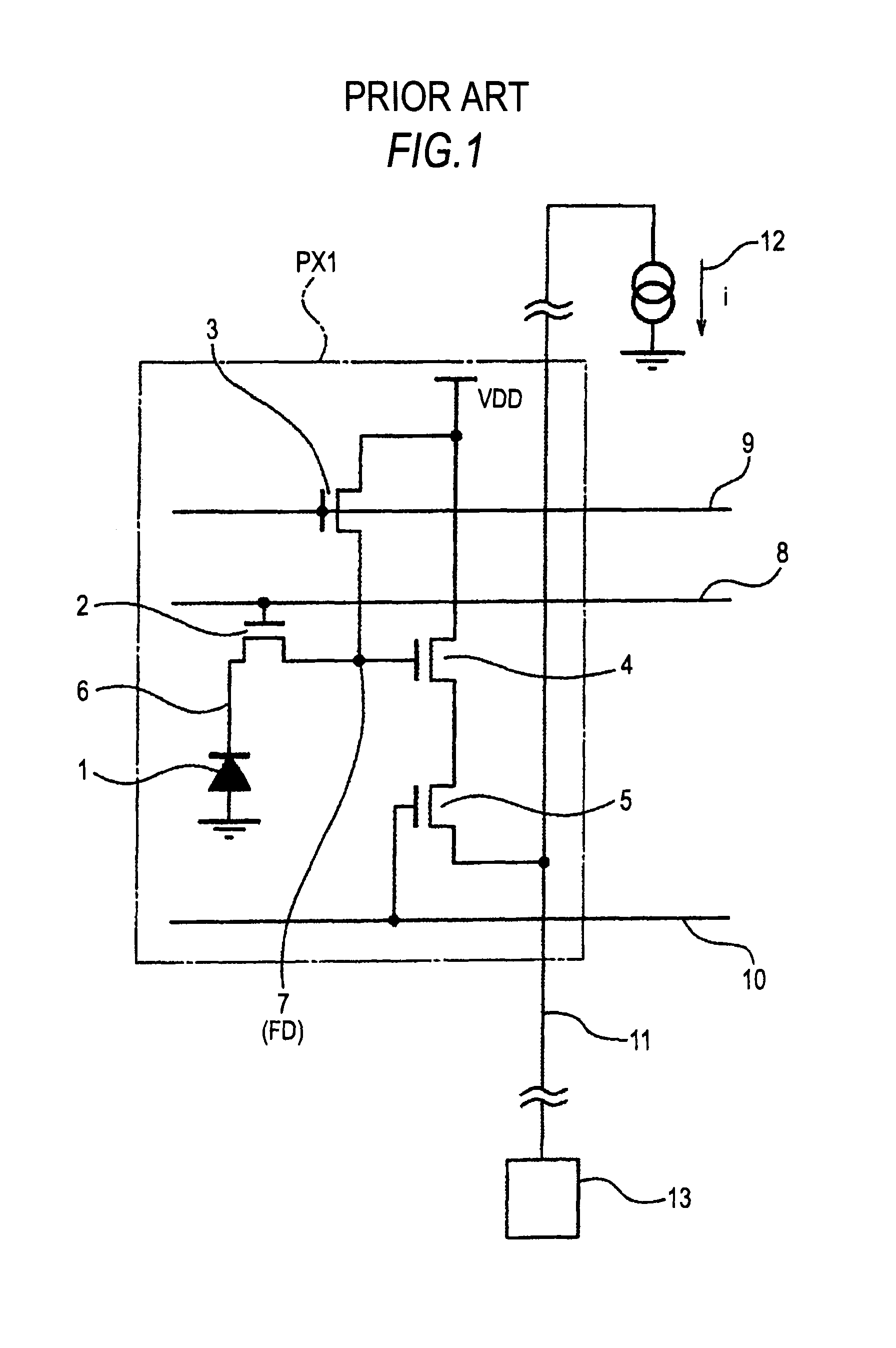
BACKGROUND OF THE INVENTION[0001]1. Field of the Invention[0002]The present invention relates to a pixel circuit, a solid-state image sensing device, and a camera system represented by a CMOS image sensor.[0003]2. Description of the Related Art[0004]Recently, CMOS imagers have widely been used for application of digital still cameras, camcorders, surveillance cameras, etc., and the market has been growing.[0005]The CMOS imager converts light entering each pixel into electrons using a photodiode as a photoelectric conversion device and accumulates them in a fixed period, and then, digitizes and outputs a signal reflecting the amount of accumulated charge to the outside.[0006]FIG. 1 shows an example of a pixel circuit containing four transistors per unit pixel.[0007]A unit pixel circuit PX1 has a photodiode 1, a transfer transistor 2, a reset transistor 3, an amp transistor 4, a selection transistor 5, an accumulation node 6, and a floating diffusion (FD) node 7.[0008]The gate electro...

Claims


Application Information

Patent Timeline
Patent Type & Authority Patents(United States)
IPC IPC(8): H04N3/14H04N5/335H01L27/00
CPCH04N5/357H04N5/3742H04N5/3745H04N5/378H01L27/14609H04N25/60H04N25/767H04N25/77H04N25/75
Inventor NISHIHARA, TOSHIYUKI
Owner SONY SEMICON SOLUTIONS CORP
Learn More