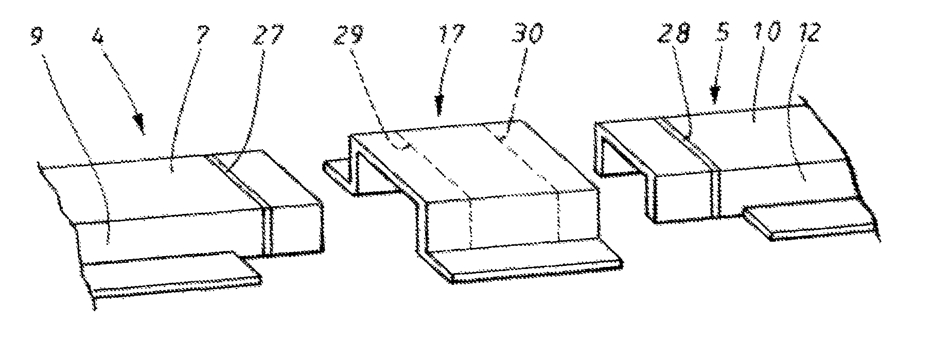
First and second U-shape waveguides joined to a dielectric carrier by a U-shape sealing frame

US8461944B2Active Publication Date: 2013-06-11TELEFON AB LM ERICSSON (PUBL)
10 Cites 0 Cited by

Patent Information

Authority / Receiving Office
US · United States
Current Assignee / Owner
Publication Date
2013-06-11

Smart Images

  • Figure 1
    Figure 1
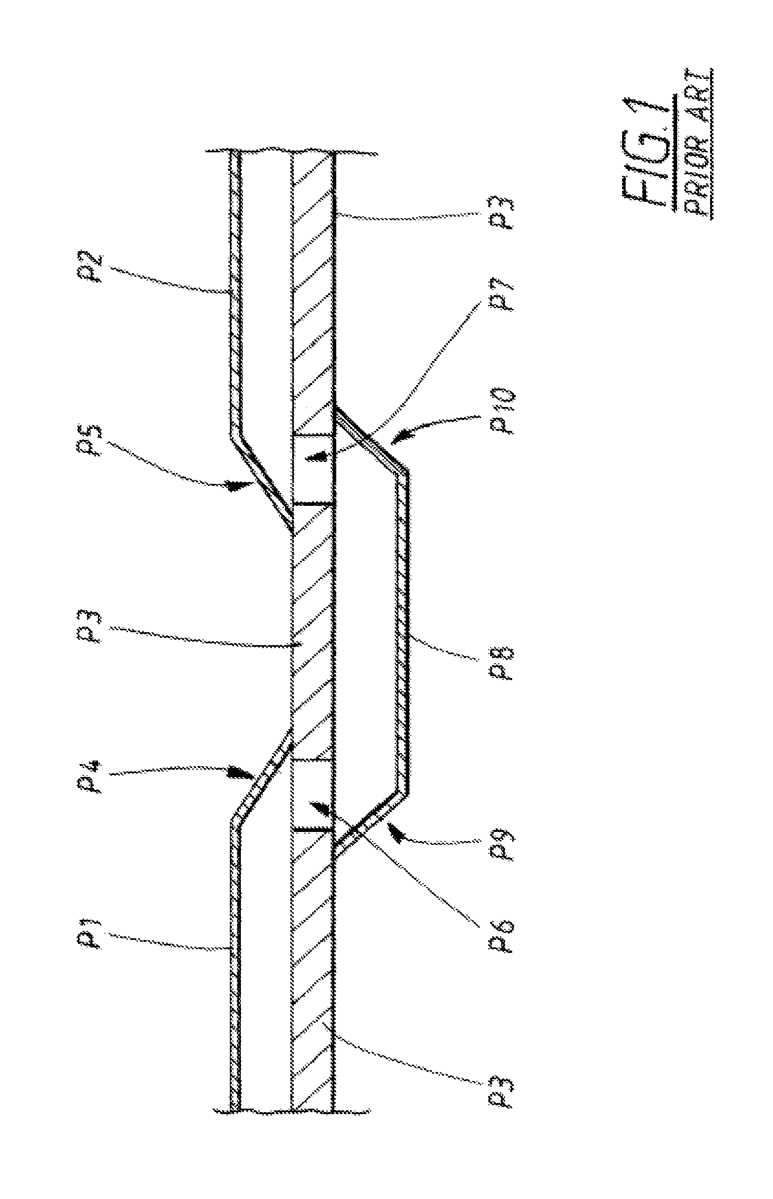
  • Figure 2
    Figure 2
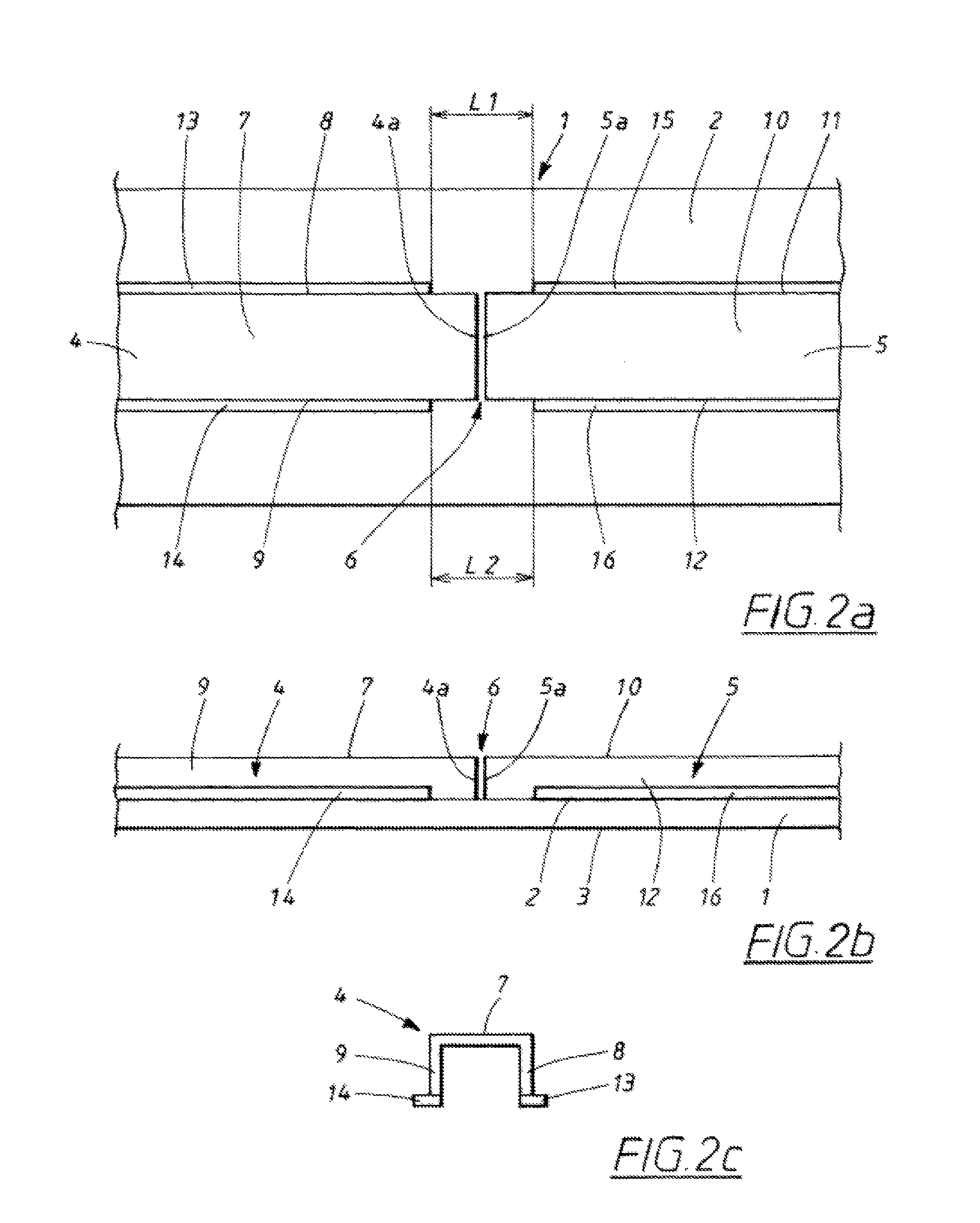
  • Figure 3
    Figure 3
Patent Text Reader

Abstract

The present invention relates to a transition arrangement comprising a first surface-mountable waveguide part and a second surface-mountable waveguide part, each of the first and second surface-mountable waveguide parts comprising a first wall, a second wall and a third wall, which second and third walls are arranged to contact a dielectric carrier material, all the walls together essentially forming a U-shape, where the first and second surface-mountable waveguide parts are arranged to be mounted on the dielectric carrier material in such a way that the first and second surface-mountable waveguide parts comprise ends which are positioned to face each other. The transition arrangement further comprises an electrically conducting sealing frame that is arranged to be mounted over and covering the ends, where the electrically conducting frame has a first wall, a second wall and a third wall, where the second and third walls are arranged to contact the dielectric carrier material, all the walls together essentially forming a U-shape.
Need to check novelty before this filing date? Find Prior Art

Description

TECHNICAL FIELD

[0001] The present invention relates to a transition arrangement comprising a first surface-mountable waveguide part and a second surface-mountable waveguide part, the first surface-mountable waveguide part comprising a first wall, a second wall and a third wall, which second and third walls are arranged to contact a dielectric carrier material, all the walls together essentially forming a U-shape, the second surface-mountable waveguide part comprising a first wall, a second wall, and a third wall, which second and third walls are arranged to contact the dielectric carrier material, all the walls together essentially forming a U-shape, where the first and second surface-mountable waveguide parts are arranged to be mounted on the dielectric carrier material in such a way that the first and second surface-mountable waveguide parts comprise ends which are positioned to face each other.

[0002] The present invention also relates to an electrically conducting sealing frame.BAC...

Examples

Embodiment Construction

[0039]In FIG. 2a and FIG. 2b, showing a respective top view and side view of a first embodiment example of the present invention, a dielectric carrier material 1 is shown, having a first main side 2 and a second main side 3 (see FIG. 2b), originally having a metallic cladding on both sides. The metallic cladding is typically comprised of a layer of copper, which optionally is covered with thin layers of other metals to enhance the electrical, mechanical, and chemical properties of the cladding. The metal on the second main side 3 is used as a ground plane, and the metal on the first main side 2 is etched away to such an extent that desired metal patterns are formed on the first main side 2. A first surface-mountable waveguide part (also referred to as a “first waveguide part”) 4 and a second surface-mountable waveguide part (also referred to as a “second waveguide part”) 5 are mounted on the dielectric carrier material 1. The respective ends 4a, 5a of the first and second surface-mo...