3-D electrically programmable and erasable single-transistor non-volatile semiconductor memory device

a non-volatile semiconductor and memory device technology, applied in the field of integrated circuits, can solve the problems of many limitations, large cost of ic fabrication facilities, and difficulty in reducing the size of devices, so as to reduce the erase voltage requirement, facilitate electron tunneling, and reduce the programming voltage requirement

Active Publication Date: 2013-06-25
SEMICON MFG INT (SHANGHAI) CORP +1
View PDF9 Cites 0 Cited by
  • Summary
  • Abstract
  • Description
  • Claims
  • Application Information

AI Technical Summary

Benefits of technology

[0016]Numerous benefits are achieved using one or more features of the present invention. In a specific embodiment, the present invention can provide a conducting channel adjacent to a stacked gate channel to supply carriers during programming, resulting in low programming voltage requirement. In some embodiments, corner structures on the floating gate facilitates electron tunneling and lowers erase voltage requirement. Lower voltage requirements make it easier to implement on-chip charge pump circuits. In certain embodiments, the device structure has a short channel length and is amenable for further scaling for improved device performance. Depending upon the specific embodiment, the invention also provides a method that is implemented using conventional process technology and equipment. Depending upon the embodiment, one or more of these benefits may be achieved. These and other benefits are described throughout the present specification and more particularly below.

Problems solved by technology

An IC fabrication facility can cost hundreds of millions, or even billions, of dollars.
Making devices smaller is very challenging, as each process used in IC fabrication has a limit.
Although fabless chip companies and foundry services have increased through the years, many limitations still exist.
For example, as logic devices are scaled and designed to operate under lower voltages, non-volatile memory devices are difficult to scale down and continue to need high voltages to operate.
For example, a conventional stacked gate non-volatile memory device requires only a single transistor for each cell, but it requires high programming current which makes it difficult to utilize on-chip high voltage generation for programming and erase.
This device can suffer from difficulty in further scaling down and low manufacturability yield.

Method used


Image

  • 3-D electrically programmable and erasable single-transistor non-volatile semiconductor memory device
  • 3-D electrically programmable and erasable single-transistor non-volatile semiconductor memory device
  • 3-D electrically programmable and erasable single-transistor non-volatile semiconductor memory device

Examples


Embodiment Construction

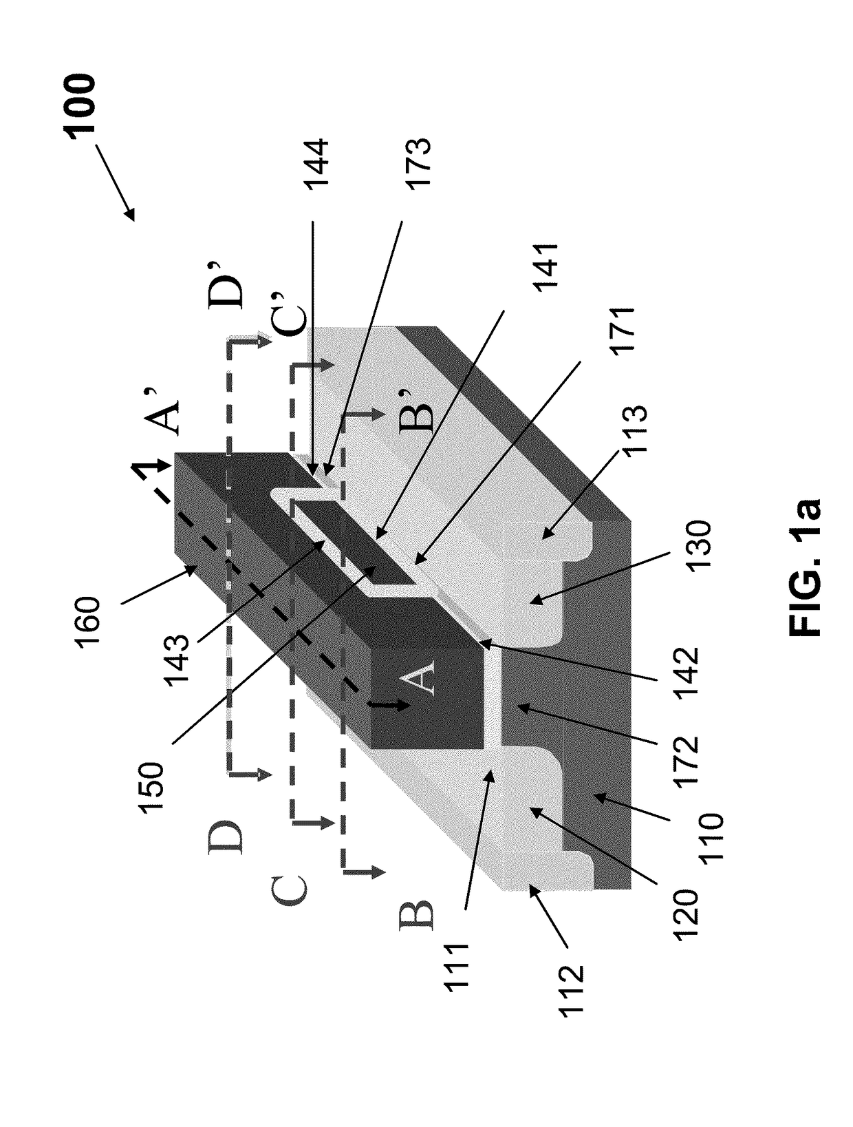
[0023]FIG. 1a is a simplified diagram of a non-volatile memory device 100 according to an embodiment of the present invention. This diagram is merely an example, which should not unduly limit the scope of the claims herein. One of ordinary skill in the art would recognize other variations, modifications, and alternatives. As shown, non-volatile memory device 100 includes a substrate 110, a surface region of the substrate 111, and isolation regions 112 and 113 in the substrate. In an embodiment, isolation regions can be shallow trench isolation (STI) regions or conventional LOCOS isolation regions, or other types of isolation regions such as junction isolation regions. Device 100 also includes a source region 120 and a drain region 130 within the substrate. In a specific embodiment, the source region and drain region are heavily doped regions. Between the source region and the drain region, device 100 also includes channel regions such as 171, 172, and 173. Each of the channel region...


PUM


Abstract

A non-volatile memory device includes a source region, a drain region, and a channel region therebetween. The channel region has a length extending from the source region to the drain region and a channel width in the direction perpendicular to the channel length direction. The device includes a floating gate positioned between the source and the drain in the channel length direction. The width of the floating gate is less than the channel width. A control gate covers a top surface and a side surface of the floating gate. The control gate also overlies an entirety of the channel region. Erasure of the cell is accomplished by Fowler-Nordheim tunneling from the floating gate to the control gate. Programming is accomplished by electrons migrating through an electron concentration gradient from a channel region underneath the control gate into a channel region underneath the floating gate and then injecting into the floating gate.

Description

CROSS-REFERENCES TO RELATED APPLICATIONS[0001]This application claims priority to Chinese Patent Application No. 200910195983.8, filed Sep. 18, 2009, commonly assigned and incorporated in its entirety by reference herein for all purposes.BACKGROUND OF THE INVENTION[0002]The present invention is directed to integrated circuits and their processing for the manufacture of semiconductor devices. More particularly, the invention provides a method and device for a non-volatile memory device including a channel region for providing carriers to a second channel region for injecting into the floating gate. Merely by way of example, the invention has been applied to embedded non-volatile memory devices having high programming efficiency and low erase voltage. But it would be recognized that the invention has a much broader range of applicability. For example, the invention can be applied to integrated circuits for stand-alone non-volatile memories or memory card applications.[0003]Integrated ...

Claims


Application Information

Patent Timeline
Patent Type & Authority Patents(United States)
IPC IPC(8): H01L29/788
CPCH01L21/28273H01L29/42324H01L29/66825H01L29/7885H01L29/40114
Inventor XIAO, DE YUANCHEN, GARYLEE, ROGER
Owner SEMICON MFG INT (SHANGHAI) CORP
Why Eureka
Try Eureka