X-ray detector and method for manufacturing the same

a technology of x-ray detector and manufacturing method, which is applied in the field of x-ray detector, can solve the problems of increasing manufacturing costs, deterioration and degradation of other components, and long time, and achieves the effects of reducing the manufacturing cost of x-ray detector, facilitating the formation of x-ray photoelectric conversion layer, and sufficient thickness

Inactive Publication Date: 2013-07-16
CANON KK
View PDF7 Cites 0 Cited by
  • Summary
  • Abstract
  • Description
  • Claims
  • Application Information

AI Technical Summary

Benefits of technology

[0019]Since polycrystalline oxides are stable, use of a polycrystalline oxide in an X-ray photoelectric conversion layer of an X-ray detector does not cause the deterioration or corrosion of other components, such as an electrode. The formation of a polycrystalline oxide sheet from a polycrystalline powder in advance facilitates the formation of an X-ray photoelectric conversion layer having a sufficient thickness. A process of producing a polycrystalline oxide powder and a process of forming a sheet from the polycrystalline oxide powder require high temperature. However, a process of forming other components on the polycrystalline oxide sheet serving as a substrate does not require high temperature.
[0020]The formation of a surface planarization layer, for example, formed of an organic substance on a surface of a polycrystalline oxide and the formation of other components, such as a storage capacitor and a TFT, on the surface planarization layer obviate the necessity of using a smooth single-crystal substrate, thereby reducing the manufacturing costs of the X-ray detector.
[0021]Electrodes disposed between the polycrystalline oxide sheets are alternately connected on the opposite sides of the polycrystalline oxide sheets. A voltage is applied between the opposite sides. Such a structure can reduce the effective thickness of a unit including a polycrystalline oxide sheet between two electrodes, that is, the interelectrode distance and increase the effective electrode area. This can reduce the interelectrode voltage. In addition, an increase in effective electrode area can improve the X-ray detectivity.
[0022]At least one high-density substance layer is disposed between layered polycrystalline oxide sheets. A pair of electrodes formed on a polycrystalline oxide sheet disposed above the high-density substance layer and another pair of electrodes formed on a polycrystalline oxide sheet disposed below the high-density substance layer are connected to their respective storage capacitors. Thus, an element including a polycrystalline oxide sheet above the high-density substance layer and an element including a polycrystalline oxide sheet below the high-density substance layer can act as independent X-ray detector elements. An X-ray detector element away from an X-ray source detects an X-ray having a shorter wavelength (high energy) than an X-ray detector element closer to the X-ray source. Thus, the comparison of the intensities of the two X-ray detector elements can yield information based on the wavelength component of the X-rays (information based on a long wavelength and information based on a short wavelength) and can yield information about the element components and the density of the analyte of the X-ray examination.

Problems solved by technology

First: A process of forming an X-ray photoelectric conversion layer takes a long period of time. In order to improve the efficiency of absorbing X-rays, an X-ray photoelectric conversion layer must have a thickness in the range of several hundreds of microns to approximately 1 mm. The formation of such a thick film by a deposition method, such as vapor deposition, requires a long period of time and possibly increases manufacturing costs. The formation of an X-ray photoelectric conversion layer by a sol-gel method requires high temperature, often resulting in the deterioration and degradation of other components and lowering the yield.
Second: Selenium or iodine in known photoelectric conversion layers often reacts with another component of the detector, such as an electrode, causing the corrosion and deterioration of the component. This also lowers the yield.
Third: Use of single crystals, such as CdTe single crystals, in the X-ray photoelectric conversion layer entails increased costs due to their very high prices.
Fourth: Use of polycrystals, such as CdTe polycrystals, to solve the third problem results in a low yield of another component, such as a thin-film transistor (hereinafter also referred to as a “TFT”), directly formed on the polycrystals because, unlike amorphous films or single crystals, the polycrystals have a rough surface. Thus, in order to improve the yield, two substrates on which a TFT and an X-ray photoelectric conversion layer are formed separately are bonded together. However, the bonding process can also increase manufacturing costs.
Fifth: The formation of an X-ray photoelectric conversion layer having a thickness in the range of several hundreds of microns to 1 mm as described above requires the application of a high voltage (in the order of several thousands of volts) to the X-ray photoelectric conversion layer.

Method used


Image

  • X-ray detector and method for manufacturing the same
  • X-ray detector and method for manufacturing the same
  • X-ray detector and method for manufacturing the same

Examples


example 1

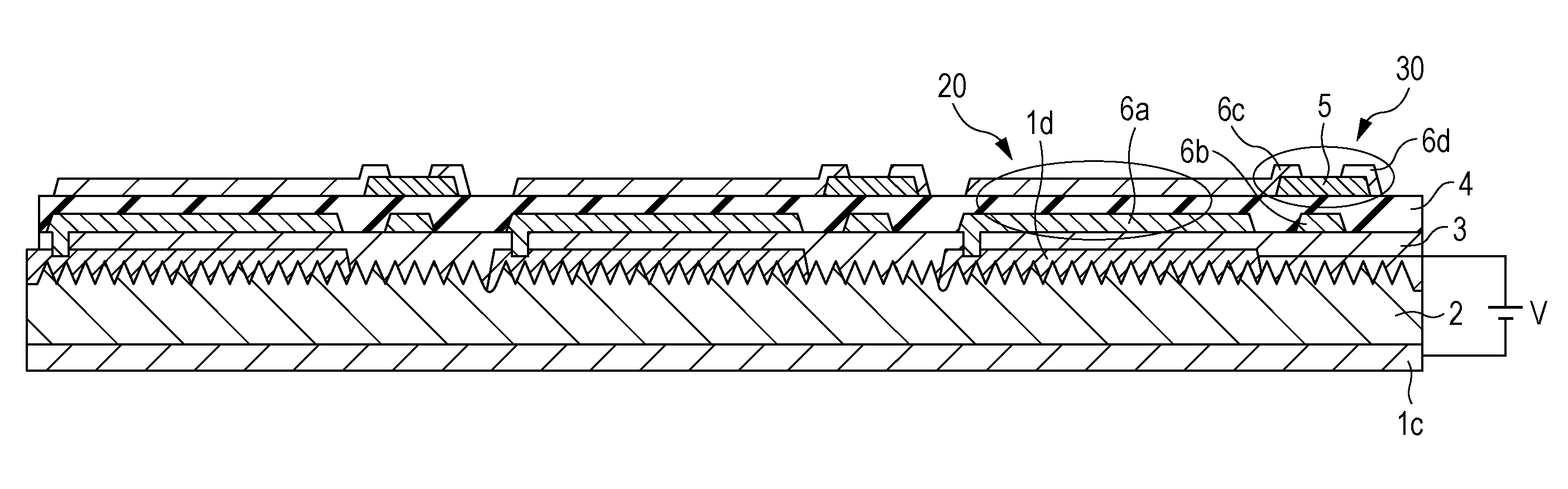
[0034]An X-ray detector array illustrated in FIG. 1 includes an X-ray photoelectric conversion layer 2, a collecting electrode 1d, a common electrode 1c, a storage capacitor 20, and a readout unit 30. The X-ray photoelectric conversion layer 2 produces electric charges in proportion to the X-ray irradiation intensity. The collecting electrode 1d collects the electric charges produced by the X-ray photoelectric conversion layer 2. The common electrode 1c is disposed on a surface of the X-ray photoelectric conversion layer 2 opposite to the collecting electrode 1d. The storage capacitor 20 stores the electric charges collected by the collecting electrode 1d. The readout unit 30 reads out the electric charges stored in the storage capacitor 20.

[0035]A voltage V is applied between the collecting electrode 1d and the common electrode 1c. The X-ray photoelectric conversion layer 2 is formed of a polycrystalline oxide.

[0036]It is desirable that the polycrystalline oxide be mainly composed ...

example 2

[0045]A polycrystalline ceramic mainly composed of zinc oxide is used as the polycrystalline oxide. In—Ga—Zn—O, Zn—Sn—O, Cd—Sn—O, or Cd—Ge—O can also be used as the polycrystalline oxide. The polycrystalline ceramic is formed into a sheet. An electrode is printed on the sheet. The sheets are stacked and sintered.

[0046]Electrodes disposed between the sheets are alternately connected on the opposite sides of the sheets. A voltage is applied between the opposite sides. For example, an electrode on a sheet is connected to an electrode on the right side, and an electrode under the sheet is connected to an electrode on the left side. In the layered sheets, the electrodes are stacked in such a staggered form.

[0047]In an example illustrated in FIG. 4, a collecting electrode 40 is disposed on a polycrystalline oxide that forms the X-ray photoelectric conversion layer 2, and a first internal electrode 41 and a second internal electrode 42 are disposed within the polycrystalline oxide of the p...

example 3

[0052]An X-ray detector array is fabricated using a layered structure in which a plurality of polycrystalline oxide sheets and a plurality of electrodes are alternately stacked.

[0053]As illustrated in FIG. 5, a common electrode 1c and a collecting electrode 1d are formed on the opposite surfaces of a polycrystalline oxide of the X-ray photoelectric conversion layer 2 (described in Example 1 with reference to FIG. 1). An internal electrode 1b and an internal electrode 1a are formed within the polycrystalline oxide of the photoelectric conversion layer 2. The internal electrode 1b is connected to the common electrode 1c, and the internal electrode 1a is connected to the collecting electrode 1d.

[0054]As illustrated in FIG. 5, the internal electrode 1a includes three electrodes, and the internal electrode 1b also includes three electrodes. The three electrodes of the internal electrode 1a and the three electrodes of the internal electrode 1b are alternately disposed. The left ends of t...


PUM


Abstract

An X-ray detector includes an X-ray photoelectric conversion layer configured to produce electric charges in proportion to X-ray irradiation incident on the layer, a collecting electrode configured to collect the electric charges produced by the X-ray photoelectric conversion layer, a common electrode disposed on a surface of the X-ray photoelectric conversion layer opposite to the collecting electrode, a storage capacitor configured to store the electric charges collected by the collecting electrode, and a readout unit configured to read out the electric charges stored in the storage capacitor. A voltage is to be applied between the collecting electrode and the common electrode. The X-ray photoelectric conversion layer is formed of a polycrystalline oxide.

Description

BACKGROUND OF THE INVENTION[0001]1. Field of the Invention[0002]The present invention relates to a detector that can detect X-ray irradiation. More particularly, the present invention relates to a detector array that can one- or two-dimensionally measure the X-ray irradiation dose.[0003]2. Description of the Related Art[0004]X-ray techniques are widely used in medical examination and industrial inspection, in which a human body or a substance is irradiated with X-rays to acquire information about the inside of the human body or the substance from the absorption contrast of penetrating X-rays. Although photographic plates and imaging plates were widely used in the past to obtain transmission X-ray images, they have recently been replaced by two-dimensional X-ray detectors, in which the penetrating X-ray intensity is converted into electronic information. X-ray detectors are classified into an indirect conversion type and a direct conversion type. In the X-ray detectors of the indirec...

Claims


Application Information

Patent Timeline
Patent Type & Authority Patents(United States)
IPC IPC(8): G01T1/24
CPCG01T1/2928H01L31/085
Inventor YABUTA, HISATOKAJI, NOBUYUKIHAYASHI, RYOWATANABE, MASATOSHIMUKAIDE, TAIHEIFUKUDA, KAZUNORI
Owner CANON KK
Why Eureka
Try Eureka