

Active device array substrate
a technology of active devices and substrates, applied in static indicating devices, instruments, non-linear optics, etc., can solve the problems of easy observation of uneven dark and bright lines or dots, excessively high display luminance or excessively low display luminance, and significant power consumption of source drivers
Active Publication Date: 2013-08-06
AU OPTRONICS CORP
View PDF15 Cites 11 Cited by
- Summary
- Abstract
- Description
- Claims
- Application Information
AI Technical Summary
Benefits of technology
The invention is an active device array substrate that prevents the issue of dropped voltage levels caused by data lines. This technology uses advanced techniques to achieve the same results as two-dot-inversion technology, while also eliminating the coupling effect caused by data lines and maintaining a consistent level of voltage. This ensures high-quality display performance when using the active device array substrate.
Problems solved by technology
As a result, power consumption of the source drivers is significant.
As such, parts of the pixels encounter issues of excessively high display luminance or excessively low display luminance, and uneven dark and bright lines or dots are observed easily.
Method used
View moreImage
Smart ImageViewing Examples

Examples
experimental example
[0062]Tests on the pixel arrangement shown in FIG. 1 are conducted with use of the test patterns 1 (sub-pixel V-stripe R, G, B, and W) and the test patterns 2 (pixel V-stripe R, G, B, and W) respectively depicted in FIG. 6A and FIG. 7A, so as to obtain waveforms of common voltage levels as indicated in FIG. 6B and FIG. 7B.
Login to View More PUM
| Property | Measurement | Unit |
|---|---|---|
| polarity | aaaaa | aaaaa |
| polarities | aaaaa | aaaaa |
| power consumption | aaaaa | aaaaa |
Abstract
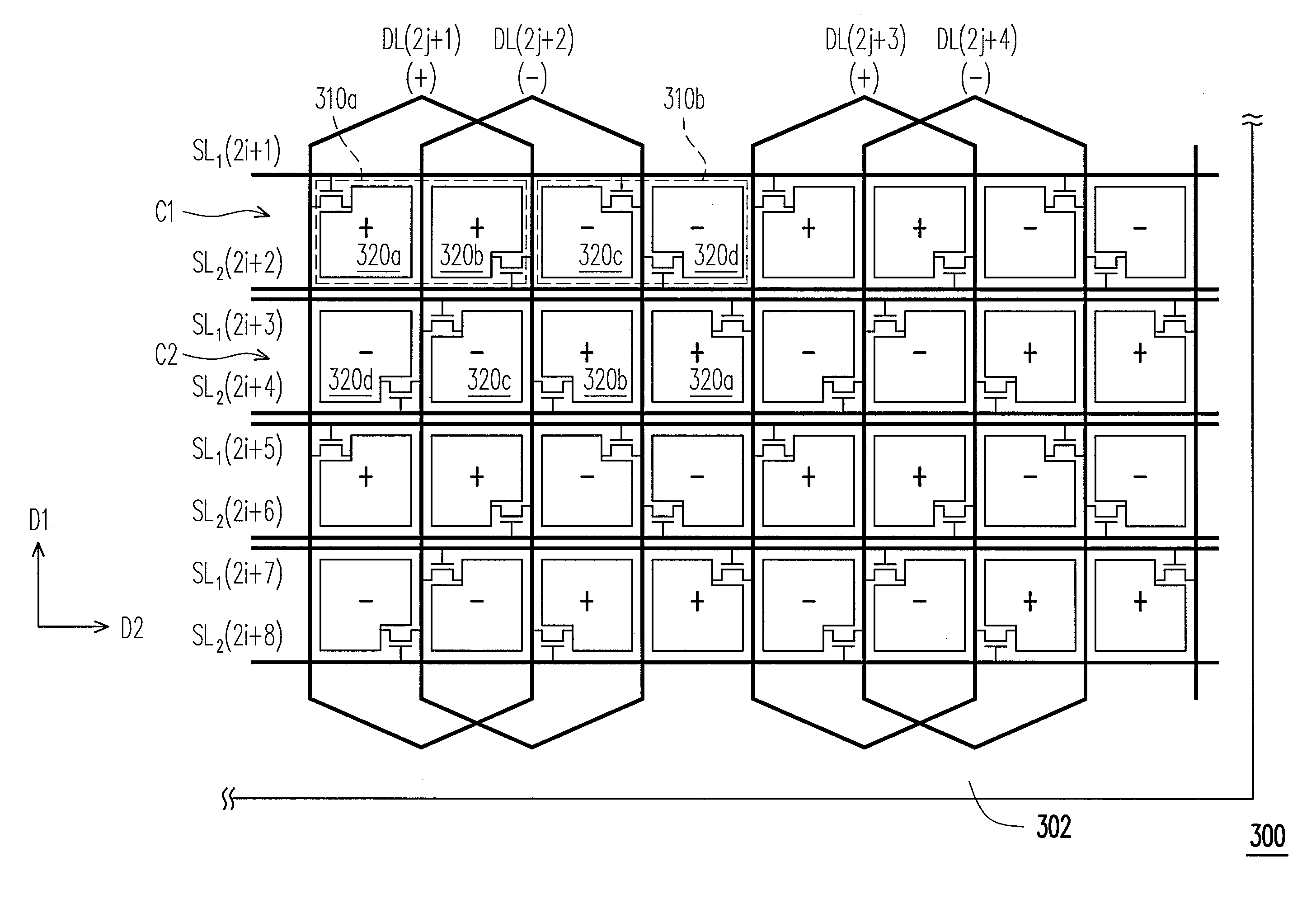
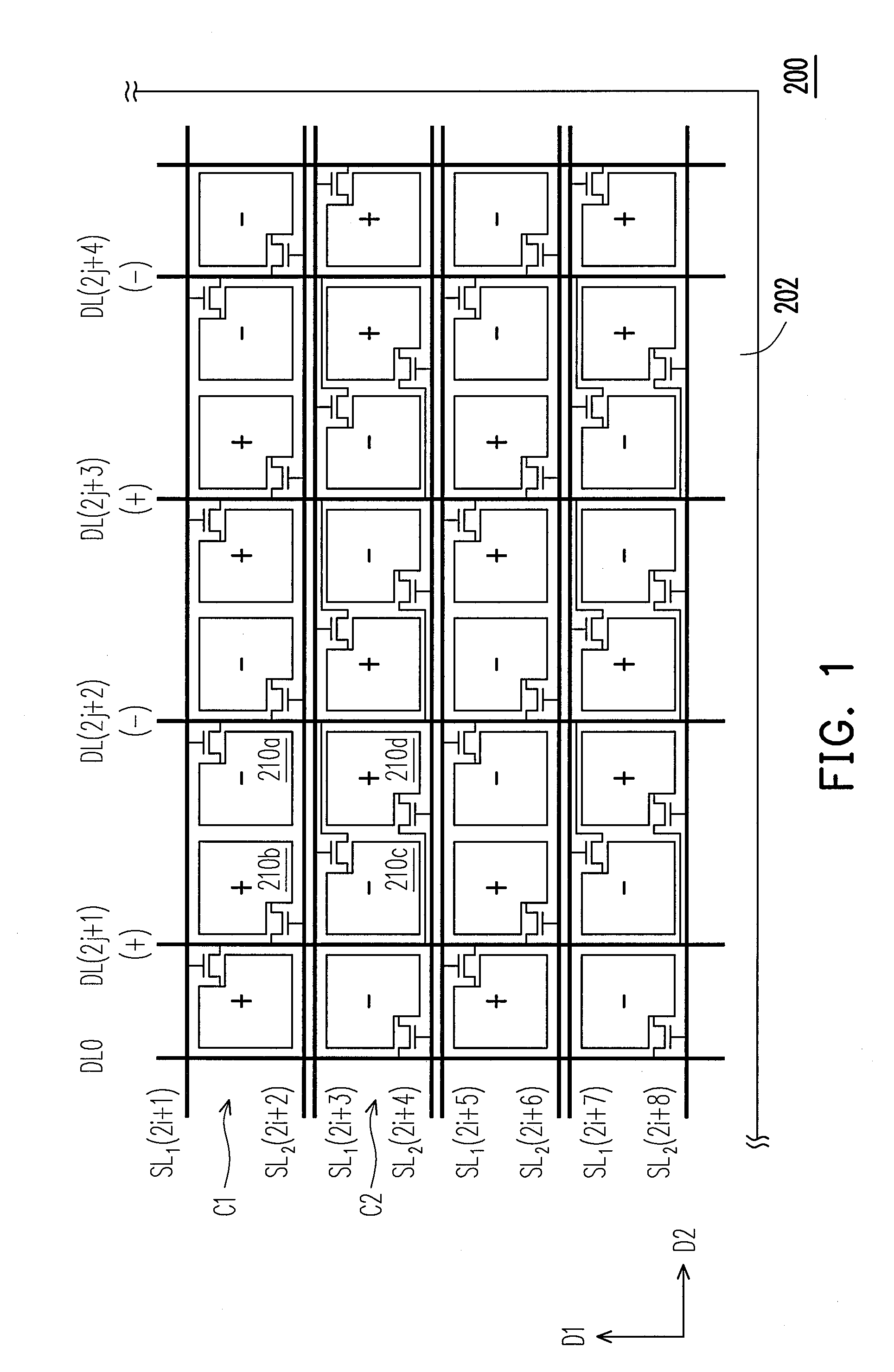
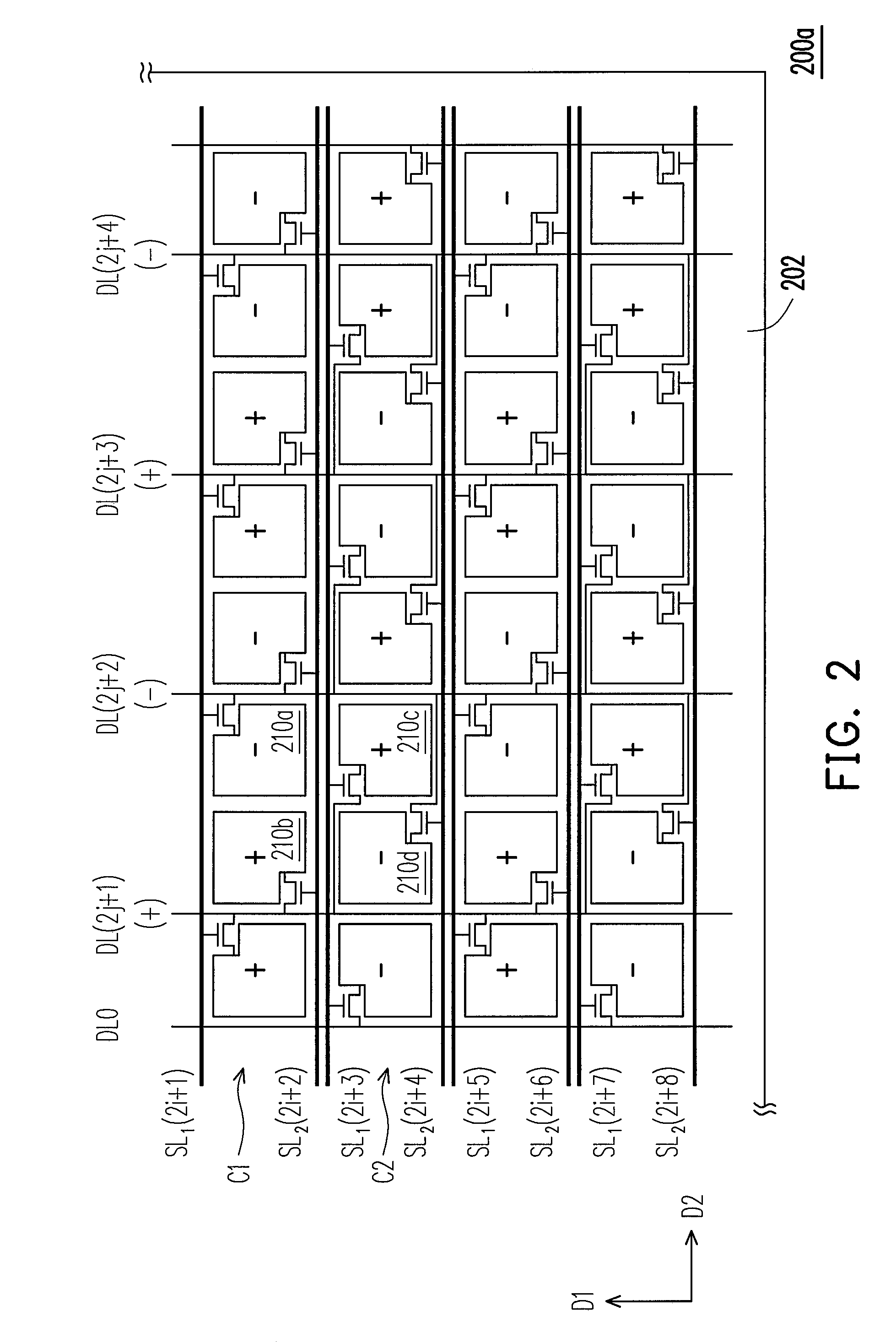
An active device array substrate includes a substrate, first scan lines, second scan lines, data lines, and pixels. The first and the second scan lines are alternately arranged along a first direction. The data lines are arranged in parallel along a second direction. The pixels are arranged to form first pixel rows and second pixel rows alternately arranged in the first direction. The first pixel row includes first and second pixels electrically connected to the first scan lines, the second scan lines, and the data line, respectively. The second pixel row includes third and fourth pixels electrically connected to the first scan lines, the second scan lines, and the data line, respectively. The pixels between two adjacent data lines are arranged in two columns. Among the pixels in the same column, the pixels in odd rows and in even rows are electrically connected to different data lines, respectively.
Description
CROSS-REFERENCE TO RELATED APPLICATION[0001]This application claims the priority benefit of Taiwan application serial no. 99116097, filed on May 20, 2010. The entirety of the above-mentioned patent application is hereby incorporated by reference herein and made a part of this specification.BACKGROUND OF THE INVENTION[0002]1. Field of the Invention[0003]The invention relates to a substrate and particularly relates to an active device array substrate.[0004]2. Description of Related Art[0005]One of the pixel array structures of existing liquid crystal display (LCD) panels is referred to as a half source driver (HSD) design. Under the HSD design, the number of scan lines is doubled, and two adjacent pixels share a data line, such that the number of the data lines and the number of required source drivers are reduced by half. Thereby, manufacturing costs of pixel arrays can be lowered down.[0006]It is noted that the LCD panel having the HSD design is driven in a dot-inversion manner or a...
Claims
Login to View More Application Information
Patent Timeline
 Patent Type & AuthorityPatents(United States)
IPC IPC(8): G02F1/1343
CPCG02F1/136286G09G3/3614G09G3/3648G09G2330/021G09G2300/0452G09G2320/0233G09G2300/0426
InventorSU, KUO-CHANGHSU, KUO-HUALIU, CHUN-HSINCHEN, YUNG-CHIH
OwnerAU OPTRONICS CORP