Polarization doping in nitride based diodes

a technology of nitride and diodes, applied in the direction of basic electric elements, electrical equipment, semiconductor devices, etc., can solve the problems of reducing the resistance of any component or layer, reducing the total series resistance of leds,

Active Publication Date: 2013-08-27
CREELED INC
View PDF145 Cites 22 Cited by
  • Summary
  • Abstract
  • Description
  • Claims
  • Application Information

AI Technical Summary

Problems solved by technology

Thus, reducing the resistance of any component or layer would also reduce the total series resistance of the LED.

Method used


Image

  • Polarization doping in nitride based diodes
  • Polarization doping in nitride based diodes
  • Polarization doping in nitride based diodes

Examples


Embodiment Construction

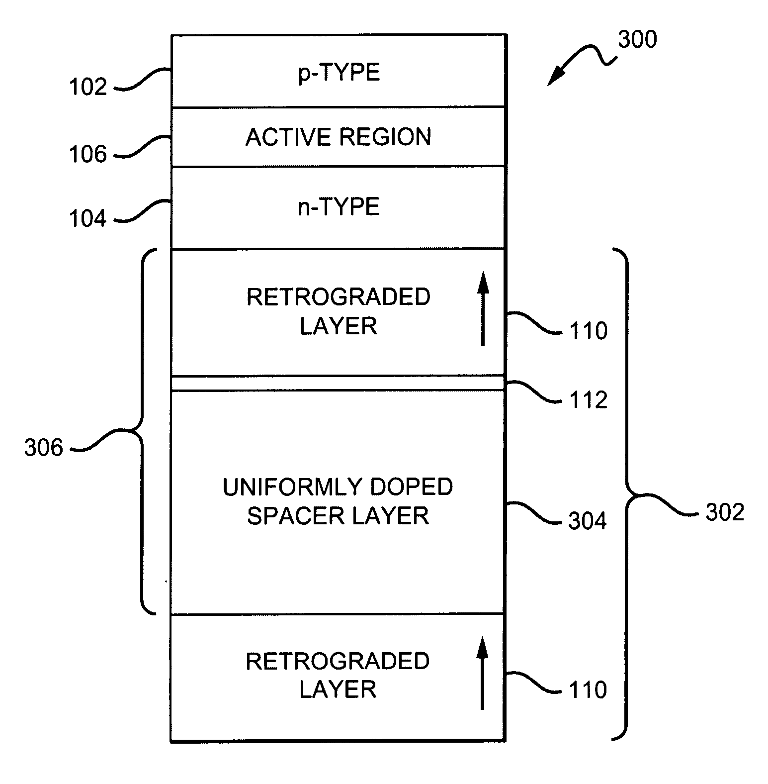
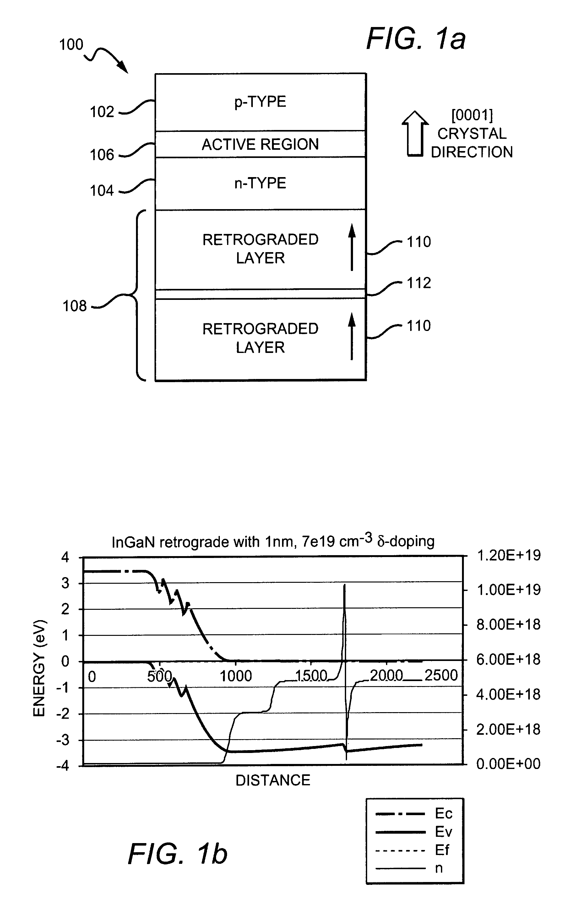
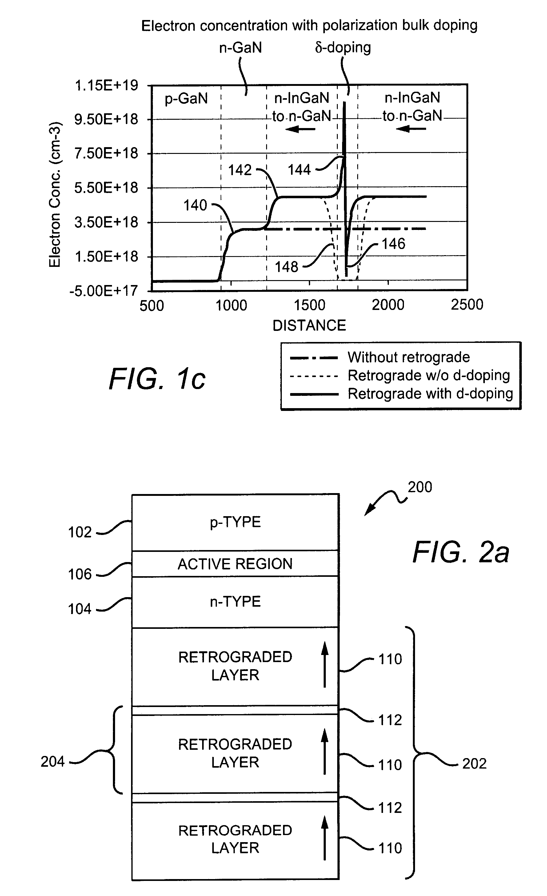
[0036]The present invention as embodied in the claims provides improved materials and material configurations for use in semiconductor devices. Although the novel structures and methods presented are useful in many different semiconductor applications, they are particularly well-suited for use in polar or semi-polar nitride-based LED systems to reduce the series resistance and the operating voltage of these devices.

[0037]The series resistance Rs of an LED can be modeled by the equation:

Rs≡Rc(n)+Rc(p)+Rb(n)+Rb(p)

where Rc(n) and Rc(p) represent the contact resistances for n- and p-contacts, respectively, and Rb(n) and Rb(P) represent the bulk resistance of the n- and p-type epitaxial layers, respectively. For example, a nominal 460 nm GaN LED has a bandgap of 2.7 eV. Assuming a lossless system, the LED would also have an operating voltage of 2.7 eV. However, in reality there are voltage penalties associated with each component contributing to the series resistance. This voltage penalt...


PUM


Abstract

A light emitting device comprising a three-dimensional polarization-graded (3DPG) structure that improves lateral current spreading within the device without introducing additional dopant impurities in the epitaxial structures. The 3DPG structure can include a repeatable stack unit that may be repeated several times within the 3DPG. The stack unit includes a compositionally graded layer and a silicon (Si) delta-doped layer. The graded layer is compositionally graded over a distance from a first material to a second material, introducing a polarization-induced bulk charge into the structure. The Si delta-doped layer compensates for back-depletion of the electron gas at the interface of the graded layers and adjacent layers. The 3DPG facilitates lateral current spreading so that current is injected into the entire active region, increasing the number of radiative recombination events in the active region and improving the external quantum efficiency and the wall-plug efficiency of the device.

Description

[0001]This invention was made with Government support under Contract No. USAF 05-2-5507. The Government has certain rights in this invention.BACKGROUND OF THE INVENTION[0002]1. Field of the Invention[0003]The invention relates generally to materials used in polar and semi-polar semiconductor devices and, more particularly, to polarization-induced bulk doping techniques to reduce the series resistance of light emitting diodes (LEDs) and improve lateral current spreading.[0004]2. Description of the Related Art[0005]Light emitting diodes (LED or LEDs) are solid state devices that convert electric energy to light, and generally comprise one or more active layers of semiconductor material sandwiched between oppositely doped layers. A bias is applied across the doped layers, injecting holes and electrons into the active layer where they recombine to generate light. Light is emitted from the active layer and from all surfaces of the LED. A typical high efficiency LED comprises an LED chip ...

Claims


Application Information

Patent Timeline
Patent Type & Authority Patents(United States)
IPC IPC(8): H01L33/30H01L33/14H01L33/32
CPCH01L33/14H01L33/32H01L29/2003
Inventor CHAKRABORTY, ARPAN
Owner CREELED INC
Why Eureka
Try Eureka