Check patentability & draft patents in minutes with Patsnap Eureka AI!

8-transistor SRAM cell design with outer pass-gate diodes

a sram cell and transistor technology, applied in transistors, digital storage, instruments, etc., can solve problems such as affecting the stability and write margin, affecting the stability of the sram cell, and compromising the variability toleran

Active Publication Date: 2013-09-03
GLOBALFOUNDRIES U S INC
View PDF23 Cites 5 Cited by
  • Summary
  • Abstract
  • Description
  • Claims
  • Application Information

AI Technical Summary

Benefits of technology

This configuration maintains write margin advantages while enabling column select writing without causing cell disturbs, ensuring data integrity during read and write operations.

Problems solved by technology

This delicate balance of transistor strength ratios can be severely impacted by device variations, which dramatically degrade stability and write margins, especially in scaled technologies.
In a 6-transistor SRAM cell, variability tolerance is compromised by the conflicting needs of cell read stability and writeability.
Because the same pass-gate devices are used to both read and write the cell, it is inevitable that the two conditions cannot be simultaneously optimized.
While the 8-transistor cell solves read stability issues, a similar problem arises during a write operation if column select functionality (also known as half-select, partial write, or masked write) is desired.
In 8-transistor SRAM, operating the memory in such a fashion would unintentionally write other bits in other columns due to the strong pass-gates employed.

Method used


Image

  • 8-transistor SRAM cell design with outer pass-gate diodes
  • 8-transistor SRAM cell design with outer pass-gate diodes
  • 8-transistor SRAM cell design with outer pass-gate diodes

Examples


Embodiment Construction

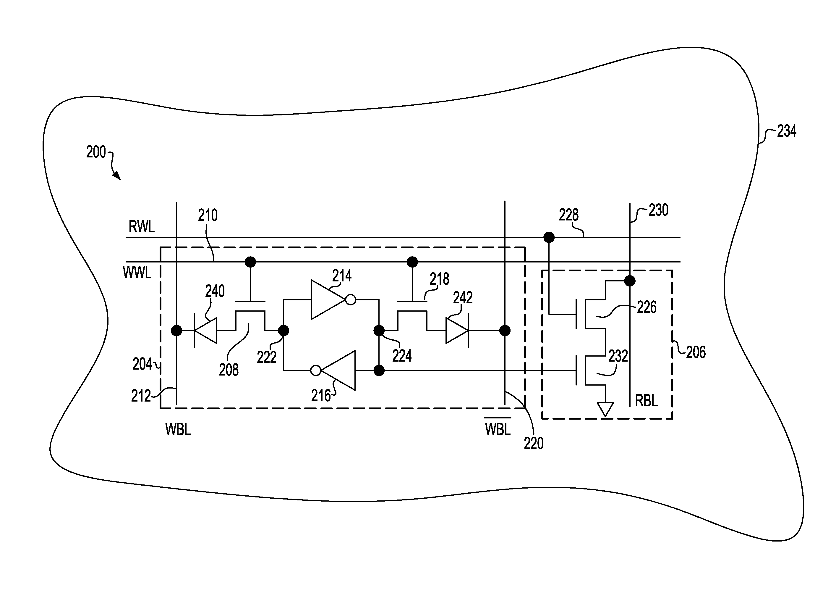
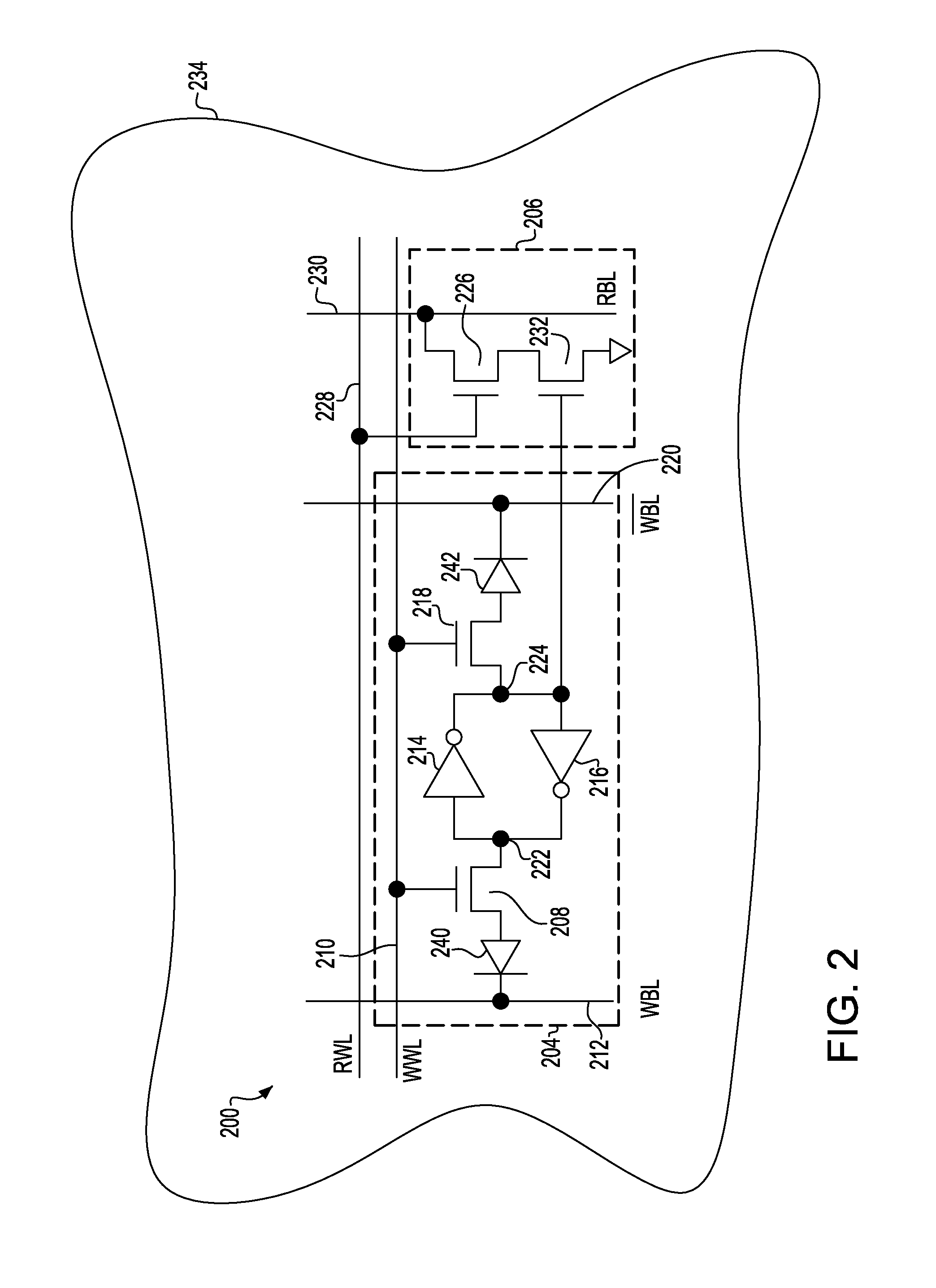
[0018]The present exemplary embodiments are directed to an 8-transistor SRAM cell in which column select writing functionality is enabled without creating cell disturbs during column select writing. In the exemplary embodiments, the pass-gates in the 8-transistor SRAM cell are altered to permit higher performance in the pull-down (write mode) configuration and lower performance in the pull-up mode, thus retaining the write margin advantage of the 8-transistor SRAM cell. By keeping the pull-up mode for the pass-gate weak, column select writing mode is permitted without disturbing adjacent bits.

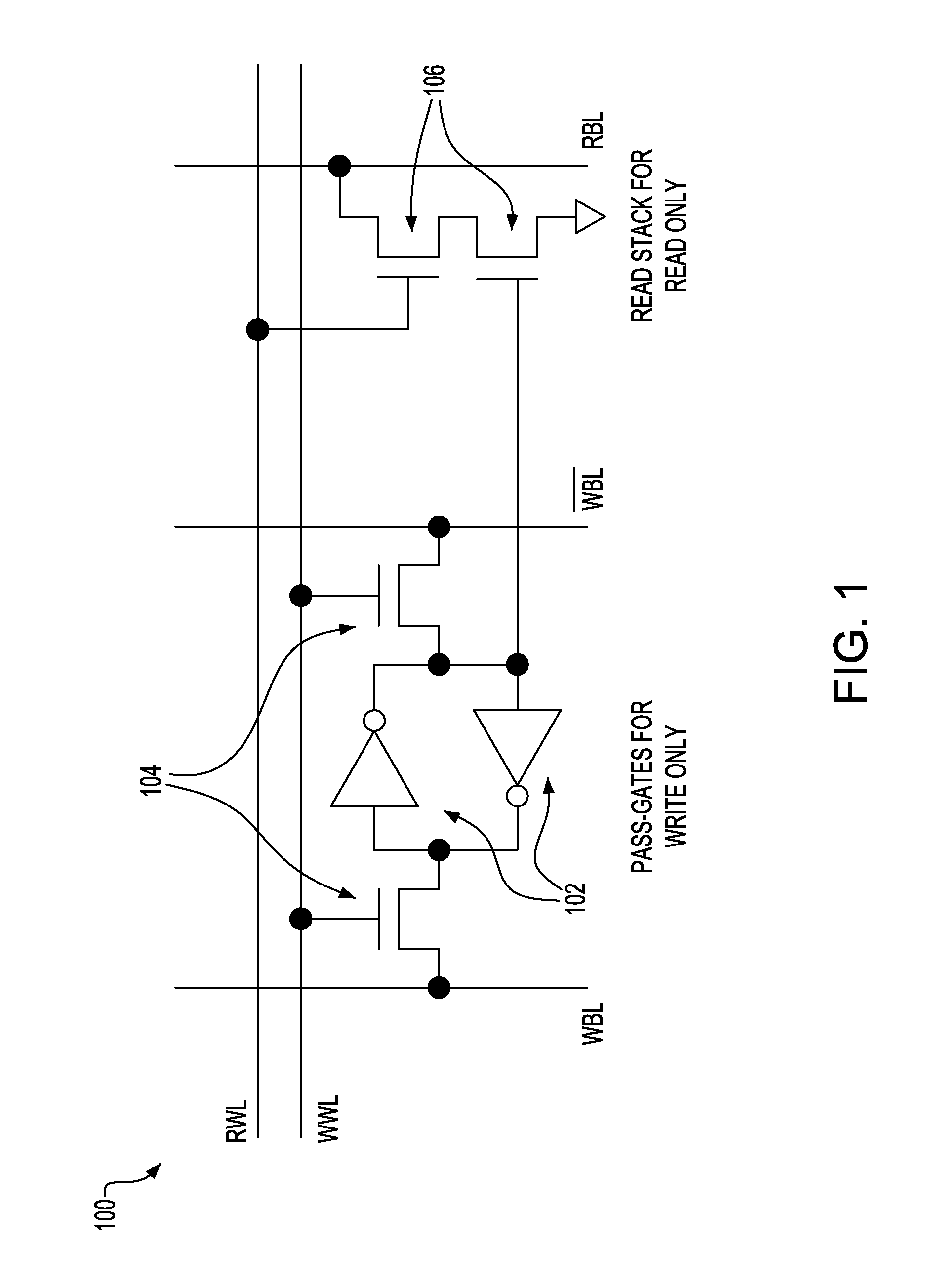
[0019]Referring to the Figures in more detail, and particularly referring to FIG. 1, there is illustrated a block diagram of an 8-transistor SRAM 100 which includes cross-coupled inverters 102 for storing a bit and pass-gates 104 for writing a bit. Bits are read through read transistors 106. As noted previously, the two read transistors 106 are added to create a disturb-free read mechanism. Sin...


PUM


Abstract

An 8-transistor SRAM cell which includes two pull-up transistors and two pull-down transistors in cross-coupled inverter configuration for storing a single data bit; first and second pass-gate transistors having a gate terminal coupled to a write word line and a source or drain of each of the pass-gate transistors coupled to a write bit line through a series outer diode between the pass-gate and the write bit line oriented to block charge transfer from the write bit line into the cell; and first and second read transistors coupled to the two pull-up and two pull-down transistors, one of the read transistors having a gate terminal coupled to a read word line and a source or a drain coupled to a read bit line. The 8-transistor SRAM cell is adapted to prevent the value of the bit stored in the cell from changing state.

Description

RELATED APPLICATION[0001]This application is related to U.S. patent application Ser. No. 13 / 345,619 entitled “8-TRANSISTOR SRAM CELL DESIGN WITH SCHOTTKY DIODES”, filed even date herewith, and U.S. patent application Ser. No. 13 / 345,629 entitled “8-TRANSISTOR SRAM CELL DESIGN WITH INNER PASS-GATE JUNCTION DIODES”, filed even date herewith, the disclosures of which are incorporated by reference herein.BACKGROUND[0002]The present invention relates to 8-transistor SRAM cell designs and, more particularly, relates to an 8-transistor SRAM cell design having outer pass-gate diodes to enable column select functionality.[0003]A static random access memory (SRAM) is a significant memory device due to its high speed, low power consumption and simple operation. Unlike a dynamic random access memory (DRAM) cell, the SRAM does not need to regularly refresh the stored data as SRAM uses bistable latching circuitry to store each bit.[0004]As variability concerns mount in future complementary metal ...

Claims


Application Information

Patent Timeline
Patent Type & Authority Patents(United States)
IPC IPC(8): G11C11/36G11C16/24
CPCG11C16/24G11C11/412H01L27/1116H01L27/1104H01L27/0207H10B10/18H10B10/12
Inventor CHANG, LELANDLAUER, ISAACLIN, CHUNG-HSUNSLEIGHT, JEFFREY W.
Owner GLOBALFOUNDRIES U S INC
Features
  • R&D
  • Intellectual Property
  • Life Sciences
  • Materials
  • Tech Scout
  • Unparalleled Data Quality
  • Higher Quality Content
  • 60% Fewer Hallucinations
Learn More