Method of manufacturing carbon cylindrical structures and biopolymer detection device

a technology of biopolymer detection and carbon cylindrical structure, which is applied in the direction of chemically reactive gas coating, crystal growth process, chemical vapor deposition coating, etc., can solve the problems of difficult to fabricate the micro-particles of catalyst metals with diameter controlled in the range of nanometers, and the method of arc discharge or laser ablation is not suited to mass production or the manufacture of integrated circuits, etc., to achieve the effect of easy diagnosis

Inactive Publication Date: 2013-09-17
FUJITSU SEMICON LTD
View PDF10 Cites 2 Cited by
  • Summary
  • Abstract
  • Description
  • Claims
  • Application Information

AI Technical Summary

Benefits of technology

[0024]It is another object of the present invention to provide a method of manufacturing carbon nanotubes, which permits carbon nanotubes with controlled diameter and / or controlled number of walls to be manufactured efficiently, and to provide single wall or multi-wall carbon nanotubes obtained by the above-mentioned manufacturing method, and having a uniform diameter and / or a uniform number of walls.
[0051]A disease diagnosis apparatus according to the present invention is a disease diagnosis apparatus comprising the biopolymer detection device according to any one of (1) to (7) above. Since this disease diagnosis apparatus comprises the above-mentioned biopolymer detection device, the content of a protein responsible for a disease in a sample as the above-mentioned target biopolymer can be quantified in a short time and the disease can be thereby diagnosed easily and specifically.

Problems solved by technology

Regardless of the methods employed for manufacturing carbon nanotubes, control of chirality, control of diameter and control of length of the carbon nanotubes are problems remaining to be solved.
Methods using arc discharge or laser ablation are not suited to mass production or to the manufacture of integrated circuits.
However, it has been found very difficult to fabricate the micro-particles of a catalyst metal with diameter controlled in the range of nanometers in accordance with the diameter of the carbon nanotubes.
It can be easily surmised that it is difficult to form the rugged structure uniformly on the surface of the metal film so as to replace the micro-particles of the catalyst metal, especially when the diameter is small.
In this method, coalescence of micro-particles takes place by collision of micro-particles with each other before they reach the substrate surface, or by diffusion of micro-particles on the substrate surface, and tends to produce secondary particles with larger diameters, so that it is difficult to produce smaller micro-particles.
Therefore, it is highly probable that the nanotubes having desired characteristics are extremely difficult to obtain.
However, SWNTs grown in arc discharge method or laser ablation method are in the form of soot and contain a large amount of impurities so that refining to high purity is difficult and selective growth on a patterned substrate is impossible.
However, this method for obtaining finer particles of a catalyst metal has a drawback that the diameter of the catalyst metal cannot be made smaller than about several nm.
In the case of above-mentioned diabetes, the disease occurs as a result of inadequate regulation of blood sugar due to an imbalance of the function and amount of a plurality of proteins interacting with each other in complicated way, such as receptors of blood sugar and enzymes that synthesize or decompose insulin in accordance with the value of blood sugar.
In conventional diagnosis of diabetes, however, there is a problem that the direct cause of the diabetes cannot be known.
At present, no established method capable of quickly determining the amount of a plurality of proteins in close functional relation with each other, as described above, is known except for the method that combines two dimensional electrophoresis with mass spectroscopy.
However, even with this method, there are problems that effective information for diagnosis and therapy of a disease cannot be obtained sufficiently and measurement cannot be carried out quickly.
However, as for proteins, there is no amplification method for proteins corresponding to the PCR method for DNA, and in addition, reactivity with a fluorescent labeling dye is different for different proteins so that it is difficult to introduce a fluorescent labeling dye uniformly to various proteins.

Method used


Image

  • Method of manufacturing carbon cylindrical structures and biopolymer detection device
  • Method of manufacturing carbon cylindrical structures and biopolymer detection device
  • Method of manufacturing carbon cylindrical structures and biopolymer detection device

Examples


example 1

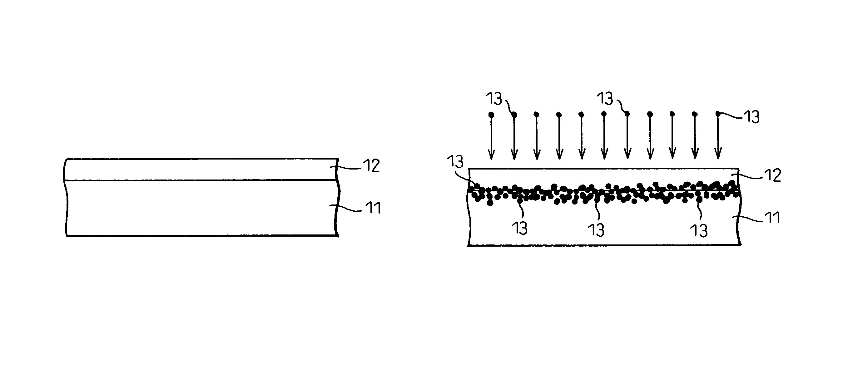
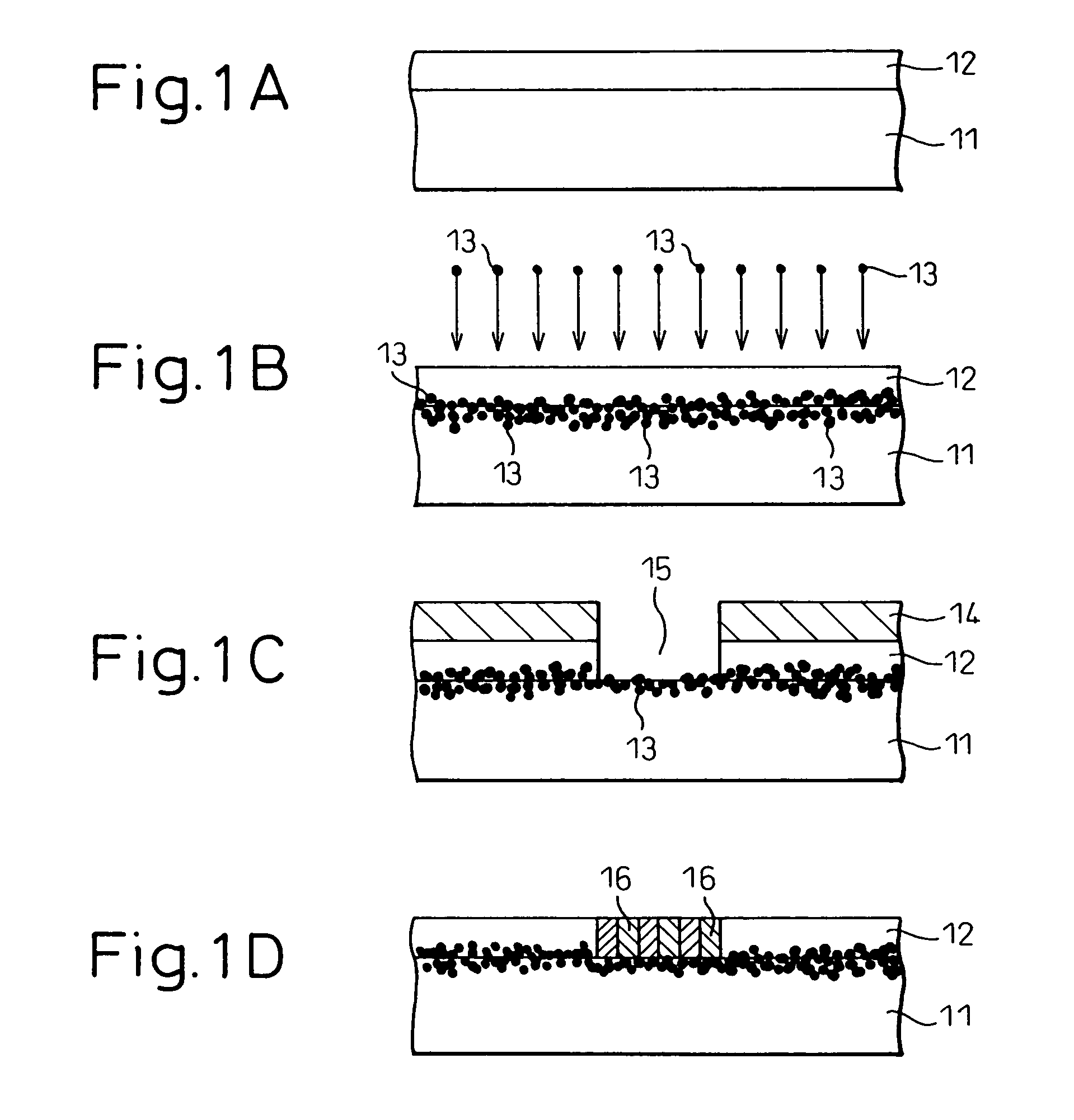
[0180]An example is described below in which carbon nanotubes were grown on a silicon substrate following the steps described with reference to FIGS. 1A to 1D.

[0181]First, a 50 nm thick SiO2 film was formed by a plasma enhanced CVD on a silicon substrate. Then, Co ions were implanted through the SiO2 film with implantation energy of 65 keV in a dose not less than 1×10¹⁶ ions / cm2. Next, a resist pattern was formed on the SiO2 film, and SF4 dry etching was performed on the SiO2 film using the resist pattern as a mask to form an opening of 0.1 to 0.5 μm in diameter for growing carbon nanotubes. After the resist pattern was removed, plasma enhanced CVD was performed at 650° C. using methane gas (acetylene gas may be used instead) and hydrogen gas at reduced pressure of about 1.33 kPa (about 10 Torr) while a DC electric field was applied in a direction perpendicular to the substrate surface to thereby grow carbon nanotubes of 50 nm in the opening.

example 2

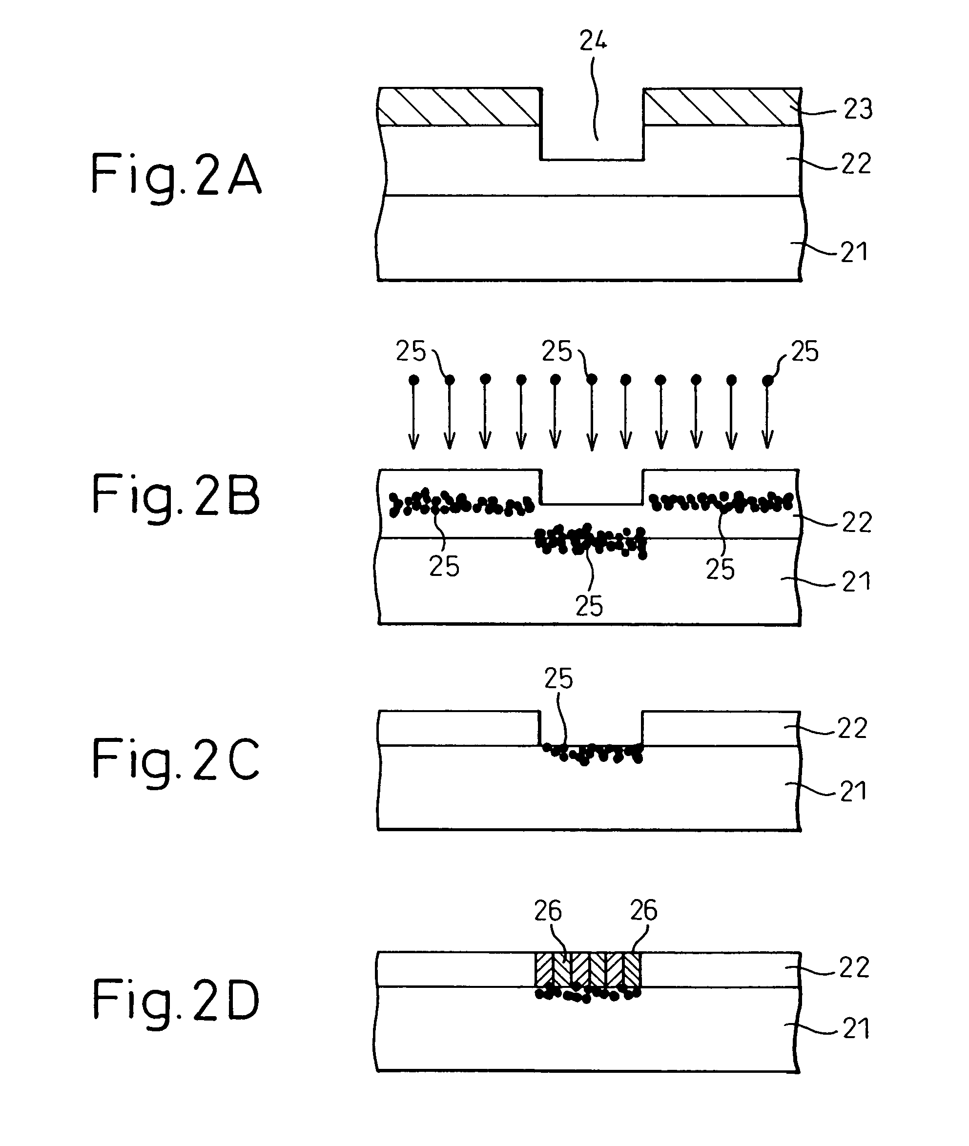
[0182]Next, an example is described below in which carbon nanotubes were grown on a silicon substrate following the steps described with reference to FIGS. 2A to 2D.

[0183]A 100 nm thick SiO2 film was formed by a plasma enhanced CVD on a silicon substrate, and a resist pattern was formed thereon. Using this resist pattern as a mask, the underlying SiO2 film was etched to midway, by controlling the duration of etching, to form a hole (recess) of 0.1 to 0.5 μm in diameter and 50 nm in depth for growing carbon nanotubes. After the resist pattern was removed, Co ions were implanted with implantation energy of 65 keV in a dose not less than 1×10¹⁶ ions / cm2. Then, anisotropic etching was performed on the SiO2 film using SF4 dry etching to dig into the SiO2 film in the hole for about 50 nm in vertical direction and to thereby expose the silicon substrate surface, while Co ions remaining in the SiO2 film in other region were removed. Then, carbon nanotubes were grown on the exposed silicon s...

example 3

[0184]In this example, as shown in FIG. 3, fullerene chemically modified with a catalyst metal was used as seed material for growing carbon nanotubes by a plasma enhanced CVD method.

[0185]First, fullerene was dispersed in water, and Ni ions and surface active agent (cyclodextrin) were added to the solution to chemically modify the fullerene with Ni.

[0186]Next, a solution of fullerene chemically modified with Ni was coated to a Si substrate (length 10 mm×width 10 mm×thickness 0.5 mm), and by patterning in a lithography method, fullerene chemically modified with Ni was disposed at optional position on the substrate to grow carbon nanotubes by a plasma enhanced CVD method.

[0187]The plasma enhanced CVD method was performed using a plasma enhanced CVD apparatus 9 as shown in FIG. 4, including a cylinder box 5 and a microwave power source 7 of 2.45 GHz as the excitation source. The substrate 8 was disposed in the vacuum chamber 3, and growth of carbon nanotubes was performed under pressur...


PUM

PropertyMeasurementUnit
diameteraaaaaaaaaa
diameteraaaaaaaaaa
sizeaaaaaaaaaa

Abstract

A method of manufacturing carbon cylindrical structures, as represented by carbon nanotubes, by growing them on a substrate using a chemical vapor deposition (CVD) method, comprising the steps of implanting metal ions to the substrate surface and then growing the carbon cylindrical structures using the metal ions as a catalyst. A method of manufacturing carbon nanotubes comprising a step of using nano-carbon material as seed material for growing carbon nanotubes is also disclosed. A biopolymer detection device comprising vibration inducing part for inducing vibration, binding part capable of resonating with the vibration induced by the vibration inducing part and capable of binding or interacting with a target biopolymer, and detection part for detecting whether or not the binding part have bound or interacted with the target biopolymer, is also disclosed.

Description

CROSS-REFERENCE TO RELATED APPLICATIONS[0001]This application is a divisional of Ser. No. 10 / 303,083, filed Nov. 25, 2002 which is based upon and claims the benefit of priority from each of prior Japanese Patent Applications No. 2001-359661, filed on Nov. 26, 2001, No. 2001-387831, filed on Dec. 20, 2001, and No. 2002-077036, filed on Mar. 19, 2002, the entire contents thereof being incorporated herein by reference.BACKGROUND OF THE INVENTION[0002]1. Field of the Invention[0003]The present invention relates to a method of manufacturing carbon cylindrical structures as represented by carbon nanotubes and, more particularly, to a method of manufacturing carbon cylindrical structures using a clean technology that is applicable to semiconductor electronics.[0004]The present invention also relates to a method of efficiently manufacturing carbon nanotubes with controlled diameter and / or number of walls, and to single wall or multi-wall carbon nanotubes which are obtained by such a manufac...

Claims


Application Information

Patent Timeline
Patent Type & Authority Patents(United States)
IPC IPC(8): D01F9/127C01B31/02C23C14/48C23C16/04C23C16/26C30B25/02G01N33/543
CPCB82Y30/00B82Y40/00C01B31/0233C23C14/48C23C16/042C23C16/26C30B25/02G01N33/54373C30B29/605C01B2202/06C01B2202/22C01B2202/36C01B32/162
Inventor AWANO, YUJIKAWABATA, AKIOFUJITA, SHOZO
Owner FUJITSU SEMICON LTD
Why Eureka
Try Eureka