
Apparatus and method for the electrolytic treatment of a plate-shaped product

a technology of electrolysis treatment and apparatus, which is applied in the direction of electrolysis coating, electrical apparatus, printed circuit manufacturing, etc., can solve the problems of insufficient uniformity of metal layer deposited, no longer possible to realise such precision structures, and new challenges for printed circuit board manufacturers with chip carriers

Active Publication Date: 2013-10-01
ATOTECH DEUT GMBH
View PDF29 Cites 1 Cited by
  • Summary
  • Abstract
  • Description
  • Claims
  • Application Information

AI Technical Summary

Benefits of technology

The purpose of this patent is to find ways to make treatment fluids act equally on work pieces, both in terms of their effect and the time it takes to achieve it. It also aims to control the treatment and make it faster. The patent looks to improve flow and mass transfer on the surface of products, including small holes, and guarantees that each surface element is supplied with fluid in a consistent way. The goal is to achieve a cost-effective design for the necessary means. Finally, the patent aims to provide an apparatus and method for electrolytic treatment of products that can achieve the aforementioned requirements for both vertical and continuous conveyorized modes.

Problems solved by technology

However, these dimensions too are only intermediate steps on the road to even smaller structures.
Based on the advancing miniaturisation of semi-conductor components, new challenges are arising for the manufacturers of printed circuit boards with chip-carriers to adapt their products to new conditions.
It is no longer possible to realise such precision structures with the necessary quality using today's conventional methods and apparatuses in printed circuit board production.
In addition, it has also been established that the uniformity of the metal layers deposited is insufficient.
This is not acceptable as the electric characteristics of the circuits produced in this way will be impaired in an unforeseeable manner, which means that the circuits will have to be thrown away.
If not, non uniform structure profiles (widths, flanks, heights) are formed setting limits to miniaturisation.
The named measures for moving the fluid have various disadvantages, the most important of which being that the fluid movement does not have the desired effectiveness with regard to the necessary uniformity of the effect of the treatment, both as regards time and also at least partially as regards location.

Method used


Image

  • Apparatus and method for the electrolytic treatment of a plate-shaped product
  • Apparatus and method for the electrolytic treatment of a plate-shaped product
  • Apparatus and method for the electrolytic treatment of a plate-shaped product

Examples


Embodiment Construction

[0012]These objects are achieved through the apparatus for the electrolytic treatment according to claim 1 and the method for the electrolytic treatment according to claim 16. Preferred specific embodiments of the invention are specified in the sub claims.

[0013]As far as the term “disposed situated opposite” is used in the description below and in the claims, this refers to a spatial relationship between the object situated opposite and the treatment surface of the product or respectively a treatment plane in which the product or respectively the treatment plane is situated. The spatial relationship is such that normal vectors extending from surface elements of the surface of the product or respectively the treatment plane in which the product is situated, meet the object disposed opposite, irrespective of whether any item is disposed between the product and the respective object or not.

[0014]As far as the terms “plate-shaped product” and “plate-shaped work pieces” are used synonymo...


PUM

PropertyMeasurementUnit
hole diameteraaaaaaaaaa

Abstract

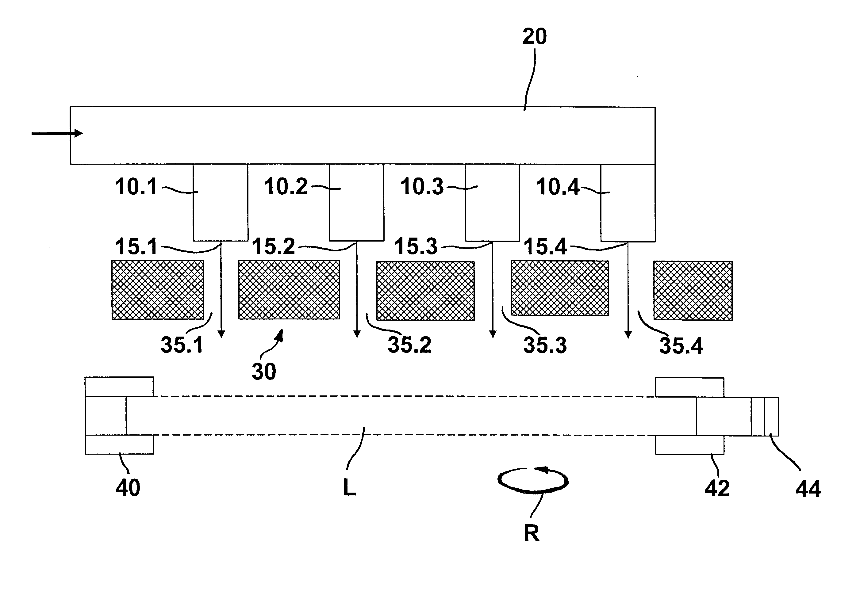
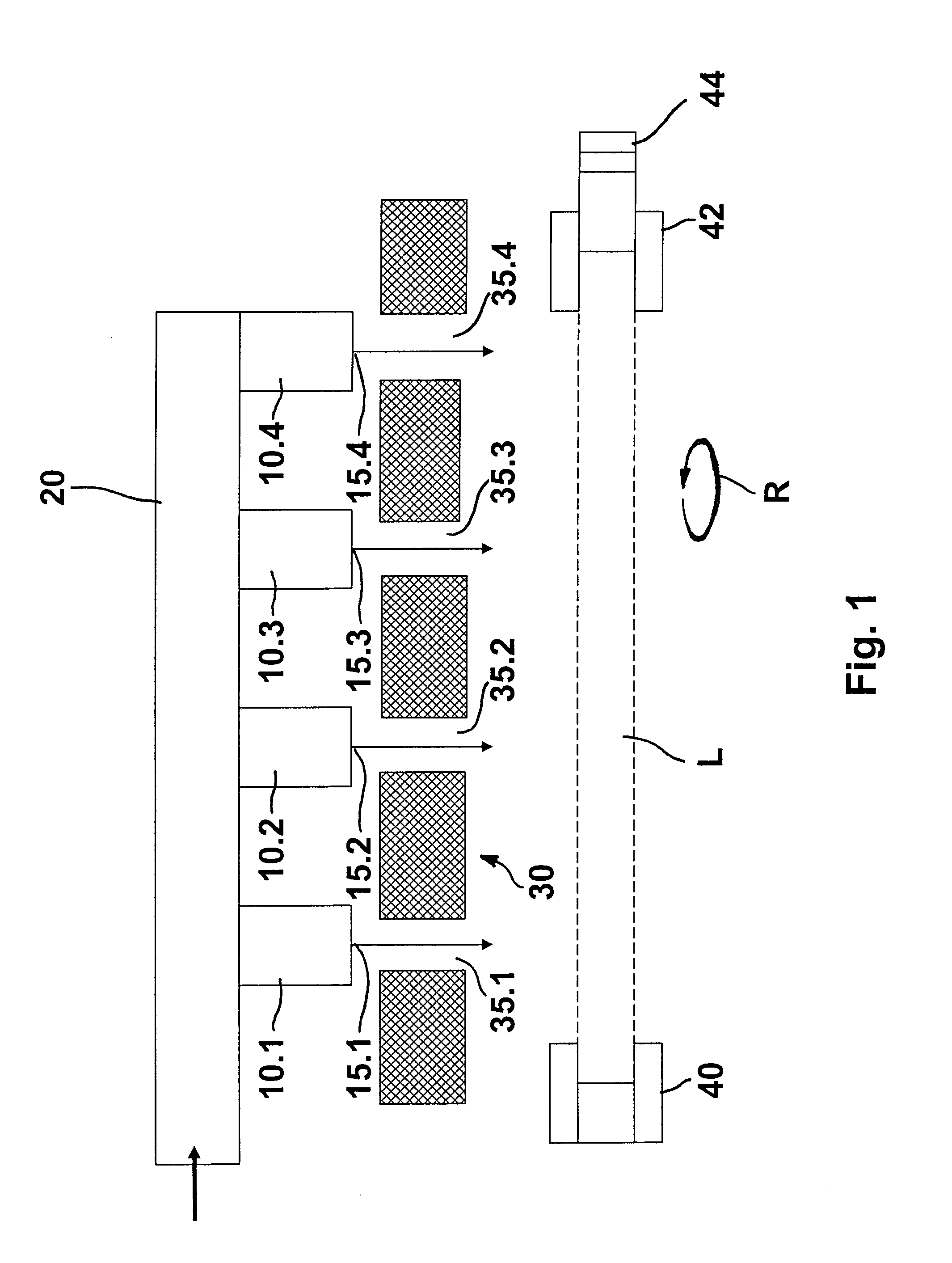
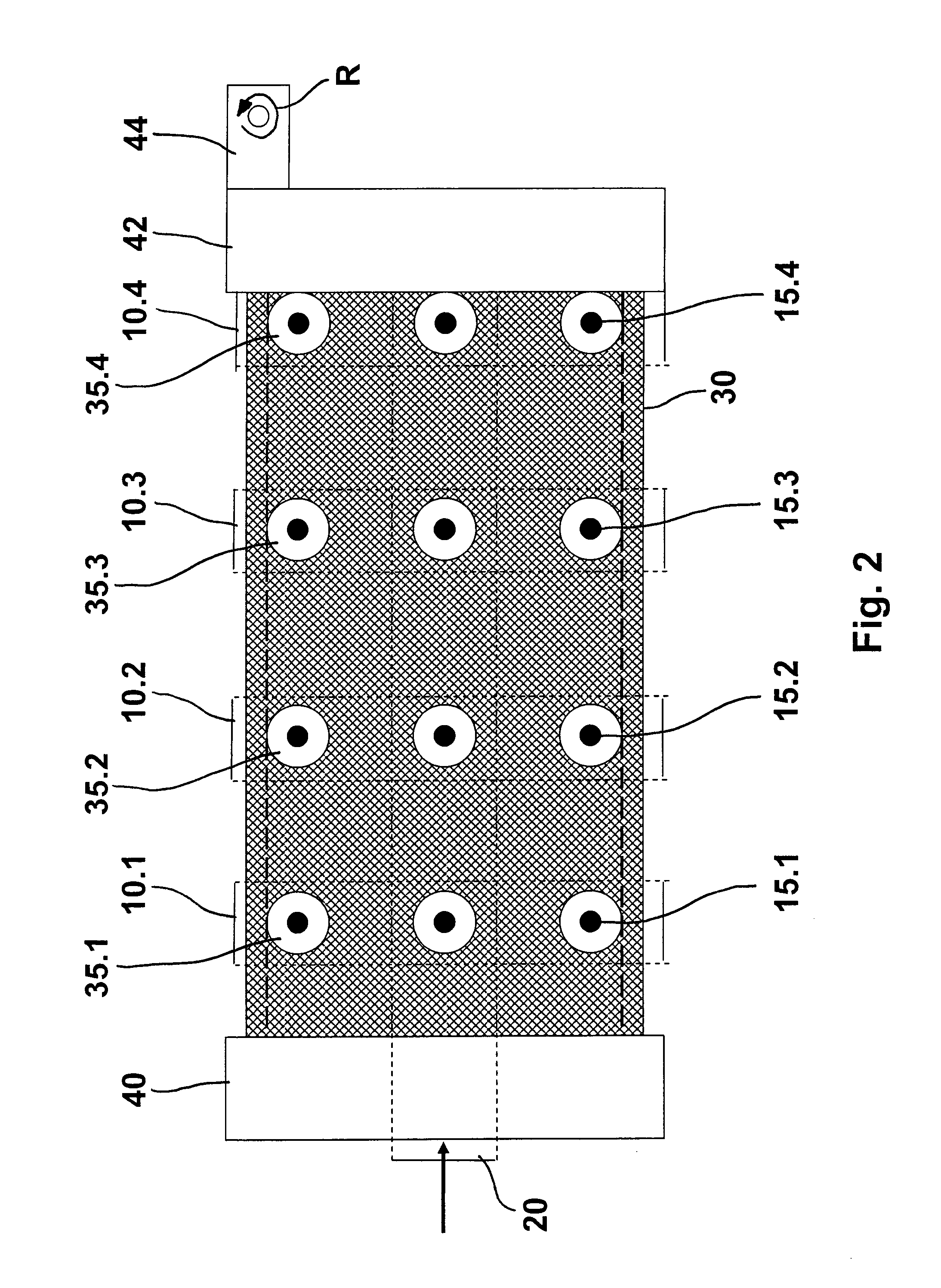
Apparatus for the electrolytic treatment of the product L using a treatment agent is used to make the treatment of a plate-shaped product more uniform. This apparatus includes devices 40, 42 for retaining the product L in the apparatus, one or more flow devices 10, which each include at least one nozzle 15 and are disposed situated opposite the product L, one or more counter electrodes 30, which are inert relative to the treatment agent and are disposed parallel to at least one treatment surface, eccentric motor means for generating a relative movement 44 between the product L, on the side, and the flow devices 10 and / or the counter electrodes 30, on the other side, in at least one direction parallel to a treatment surface. The product L can be immersed in the treatment agent during treatment.

Description

FIELD OF THE INVENTION[0001]The present invention relates to an apparatus and a method for the electrolytic treatment of a plate-shaped product that is disposed in the apparatus. Such apparatuses and methods can be used both in the production of printed circuit boards and printed circuit foils and also in the production of semiconductor wafers, solar cells, photoelectric cells and monitor plates.BACKGROUND OF THE INVENTION[0002]At present chip producers in the semi-conductor industry are working on the introduction of so-called 65-nanometer structures (Computertechnik (10), 2007). Even smaller structures of 45 nm are in the process of being developed. However, these dimensions too are only intermediate steps on the road to even smaller structures. Based on the advancing miniaturisation of semi-conductor components, new challenges are arising for the manufacturers of printed circuit boards with chip-carriers to adapt their products to new conditions. This means, for example, that cur...

Claims


Application Information

Patent Timeline
Patent Type & Authority Patents(United States)
IPC IPC(8): C25D5/04C25D5/08C25D21/10C25D17/02C25D17/06C25D7/12
CPCC25D5/04C25D5/08C25D21/10H05K3/241H05K2203/0746H05K2203/1509C25D17/001C25D7/00
Inventor SCHNEIDER, REINHARDKUNZE, HENRYWIENER, FERDINAND
Owner ATOTECH DEUT GMBH
Learn More