Printed circuit board using bump and method for manufacturing thereof

a printed circuit board and bump technology, applied in the direction of printed circuit manufacturing, printed circuit aspects, burial vaults, etc., can solve the problems of reducing the thickness of the board to be used, the difficulty of ensuring an interlayer electrical connection and a degree of freedom, etc., to achieve excellent heat dissipation effect, easy joining, and reduced manufacturing time

Inactive Publication Date: 2013-10-08
SAMSUNG ELECTRO MECHANICS CO LTD
View PDF8 Cites 1 Cited by
  • Summary
  • Abstract
  • Description
  • Claims
  • Application Information

AI Technical Summary

Benefits of technology

[0013]The present invention further provides a method for manufacturing a printed circuit board and a print circuit board manufactured thereby, which can resist against pressure of paste bumps produced during stacking due to the increased strength of a core board, be easy to join between layers, provide excellent heat-releasing effect, and be capable of collectively stacking of core boards, which was not possible with conventional methods.
[0014]The present invention further provides a method for manufacturing a printed circuit board and a print circuit board manufactured thereby, in which the manufacturing time can be reduced due to continuing work through parallel processes of plating and a process for forming window portions to form blind via holes can be omitted.

Problems solved by technology

However, the conventional manufacturing process for multilayer printed circuit boards is unable to comply to requests for low costs according to lowering prices in the applied products (e.g. cell phones, etc.) and requests for reduced lead times for increased productivity, and thus there is a demand for a new manufacturing process that can resolve such problems.
This, however, implements all-layer IVH's with only the paste bump board so that it has a weak structure and there is also a limit to reducing thickness of the board to be used as an inner layer core board due to limitation of the processing of through holes.
Also, there is a difficulty of guaranteeing an interlayer electrical connection and a degree of freedom to improve the performance of HDI or BGA boards and provide excellent heat-releasing effect.

Method used


Image

  • Printed circuit board using bump and method for manufacturing thereof
  • Printed circuit board using bump and method for manufacturing thereof
  • Printed circuit board using bump and method for manufacturing thereof

Examples


Embodiment Construction

[0037]Embodiments of the printed circuit board using bumps and manufacturing method thereof, according to aspects of the invention, will be described below in more detail with reference to the accompanying drawings.

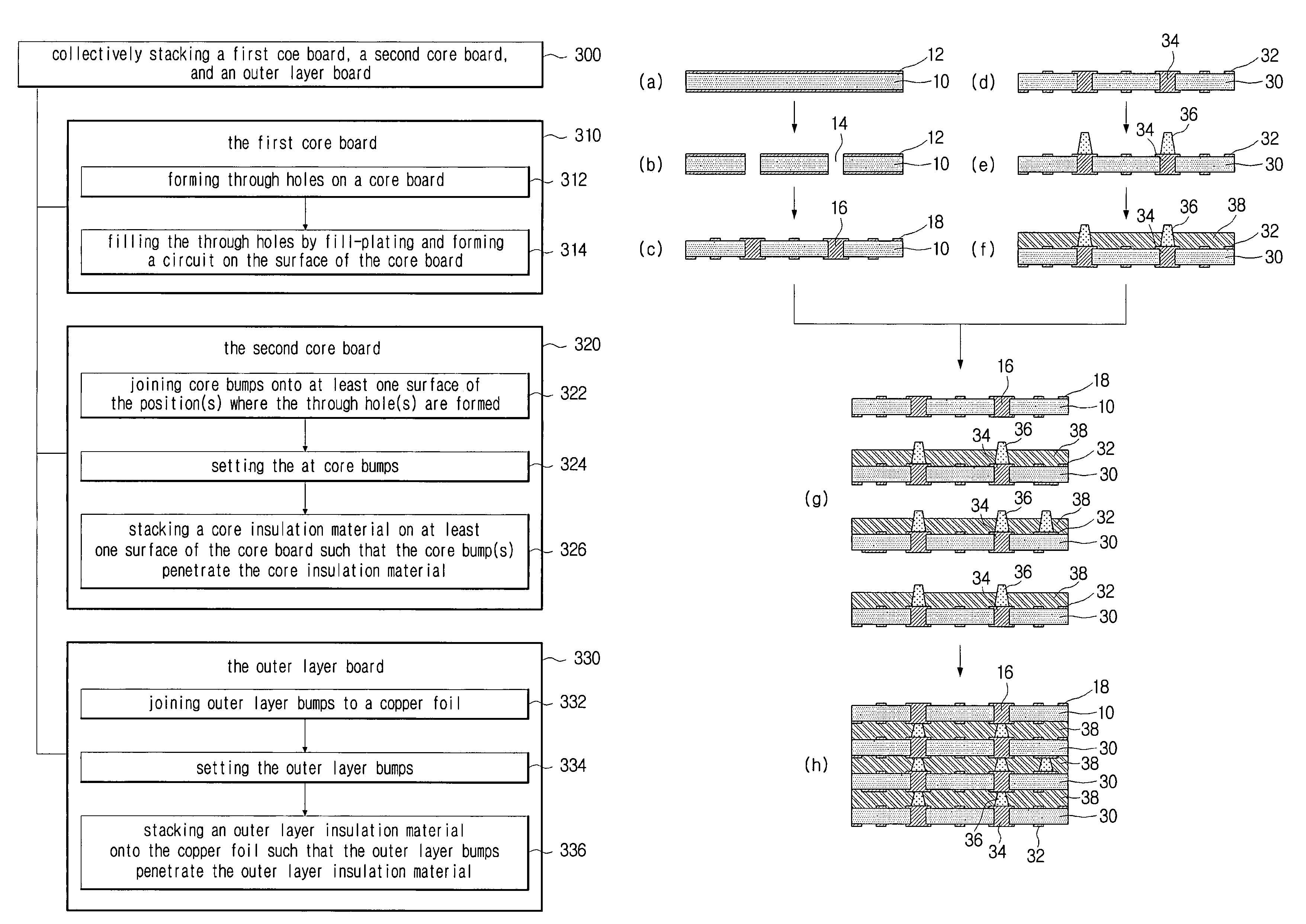
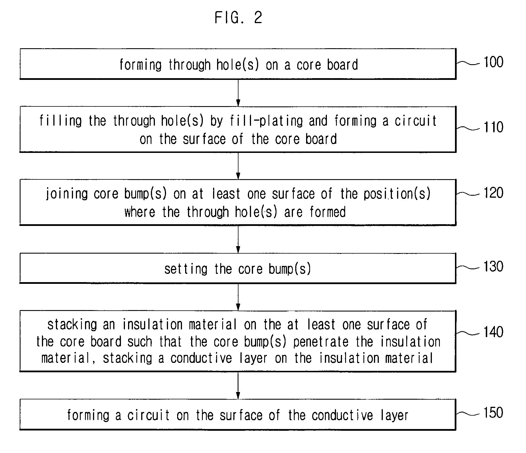
[0038]FIG. 2 is a flowchart illustrating a method of manufacturing a printed circuit board using bumps according to an embodiment of the present invention.

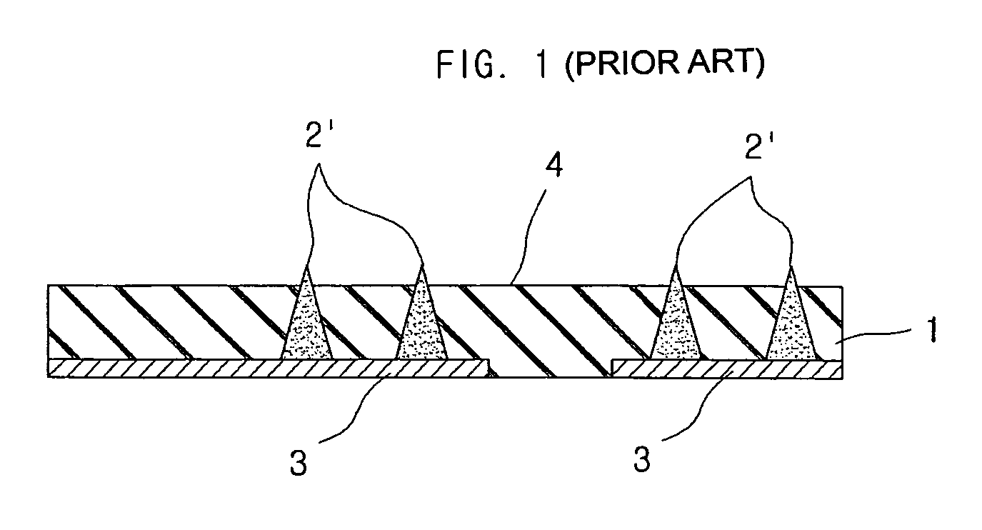
[0039]The present invention provides a core board which allows collectively manufacturing a multi-layer printed circuit board by forming through holes in the core board, filling the through holes by reverse pulse plating, printing core bumps in correspondence with the positions of the through holes, and stacking an insulation material. Accordingly, the printed circuit board may be formed, which allows forming a thick core board and forming bumps on the thick insulation layer, endures against pressure produced during the stacking process, is convenient for joining layers, exhibits excellent heat-releasing effect, allows ...


PUM

PropertyMeasurementUnit
thicknessaaaaaaaaaa
thicknessaaaaaaaaaa
thicknessaaaaaaaaaa

Abstract

The present invention provides a method for manufacturing a printed circuit board and a print circuit board manufactured thereby, in which through holes of a core board are filled by reverse pulse plating so that it allows to manufacture a core board having greater than 100 μm of a thickness which has been a processing limitation with conventional technologies and form bumps on a thick insulation layer, which has been difficult till now, and thus providing resistance against pressure of paste bumps produced during stacking due to the increased strength of a core board, convenience to join between layers, excellent heat-releasing effect, and collectively stacking of core boards, which was not possible with conventional methods.

Description

CROSS-REFERENCE TO RELATED APPLICATIONS[0001]This application claims the benefit of Korean Patent Application No. 2006-32635 filed with the Korea Industrial Property Office on Apr. 11, 2006, the disclosure of which is incorporated herein by reference in their entirety.BACKGROUND[0002]1. Technical Field[0003]The present invention relates to a printed circuit board using bumps and a manufacturing method thereof, and more particularly, to a printed circuit board formed by collectively stacking multilayer and a manufacturing method thereof.[0004]2. Description of the Related Art[0005]A conventional multilayer printed circuit board has been prepared by forming inner layer circuits on the surface of a core board, such as copper clad laminate (CCL), etc., through the application of an additive method or a subtractive method, and by forming outer layer circuits through stacking of insulation layers and metal layers in order, by the same method as for forming the inner layer circuit.[0006]Wi...

Claims


Application Information

Patent Timeline
Patent Type & Authority Patents(United States)
IPC IPC(8): H01K3/10
CPCH05K3/462H05K3/4647H05K3/4069H05K3/423H05K3/4623Y10T29/49165H05K3/4652H05K2201/09563H05K2203/0733H05K2203/1492E04H13/00
Inventor SHIN, HEE-BUMPARK, DONG-JINMOK, JEE-SOOBAE, JONG-SUKKIM, KI-HWAN
Owner SAMSUNG ELECTRO MECHANICS CO LTD
Why Eureka
Try Eureka