Driver for display panel and image display apparatus

a technology for display panels and display panels, applied in static indicating devices, instruments, optics, etc., can solve the problems of hardly satisfied space saving requirements, achieve the effect of reducing voltage drop in power source lines of display panels, preventing the generation of uneven luminance, and simplifying the wiring structure of display panels

Active Publication Date: 2013-11-19
INNOLUX CORP
View PDF27 Cites 4 Cited by
  • Summary
  • Abstract
  • Description
  • Claims
  • Application Information

AI Technical Summary

Benefits of technology

[0031]According to the driver for driving a display panel of the present invention, the control pads and the power source pads are arranged together in line, and the order of arrangement of the control pads and the power source pads is symmetrical with respect to the direction of pad arrangement. Hence, when the drivers for display that constitute a driver pair are arranged on the sides of the display panel, both ends of each power source line of the display panel can be connected to the power source pads of the drivers, respectively. Each driver is connected to different control lines. Thus, the voltage drop in the power source lines of the display panel can be reduced, the generation of uneven luminance can be prevented. Further, simplification of the wiring structure of the display panel is achievable, and space saving can be realized.
[0032]Still further, according to the driver for a display panel of the present invention, the control pads, the spare control pads, and the power source pads are arranged together in line, and if the control pads and the spare control pads are collectively labeled as the control pads, the order of arrangement of the control pads and the power source pads is symmetrical with respect to the direction of pad arrangement. Hence, when the drivers for display that constitute a driver pair are arranged respectively on the sides of the display panel, both ends of each power source line of the display panel can be connected to the power source pads of the drivers, respectively. Each driver is connected to different control lines. Thus, the voltage drop in the power source lines of the display panel can be reduced, the generation of uneven luminance can be prevented. Further, simplification of the wiring structure of the display panel is achievable, and space saving can be realized.
[0033]Still further, according to the image display apparatus of the present invention, the drivers that constitute a driver pair are respectively connected to both ends of each power source line of the display panel, whereas each driver unit is connected to different control lines. Thus, the voltage drop in the power source line can be reduced. Further, the generation of uneven luminance can be prevented, simplification of the wiring structure of the display panel is achievable, and the space saving can be realized.

Problems solved by technology

Commonly used flat-type display is a liquid crystal display, which however is not immune to problems such as a narrow viewing angle and unfavorable response characteristics.
Thus, requirement of space saving is hardly satisfied.

Method used


Image

  • Driver for display panel and image display apparatus
  • Driver for display panel and image display apparatus
  • Driver for display panel and image display apparatus

Examples


first embodiment

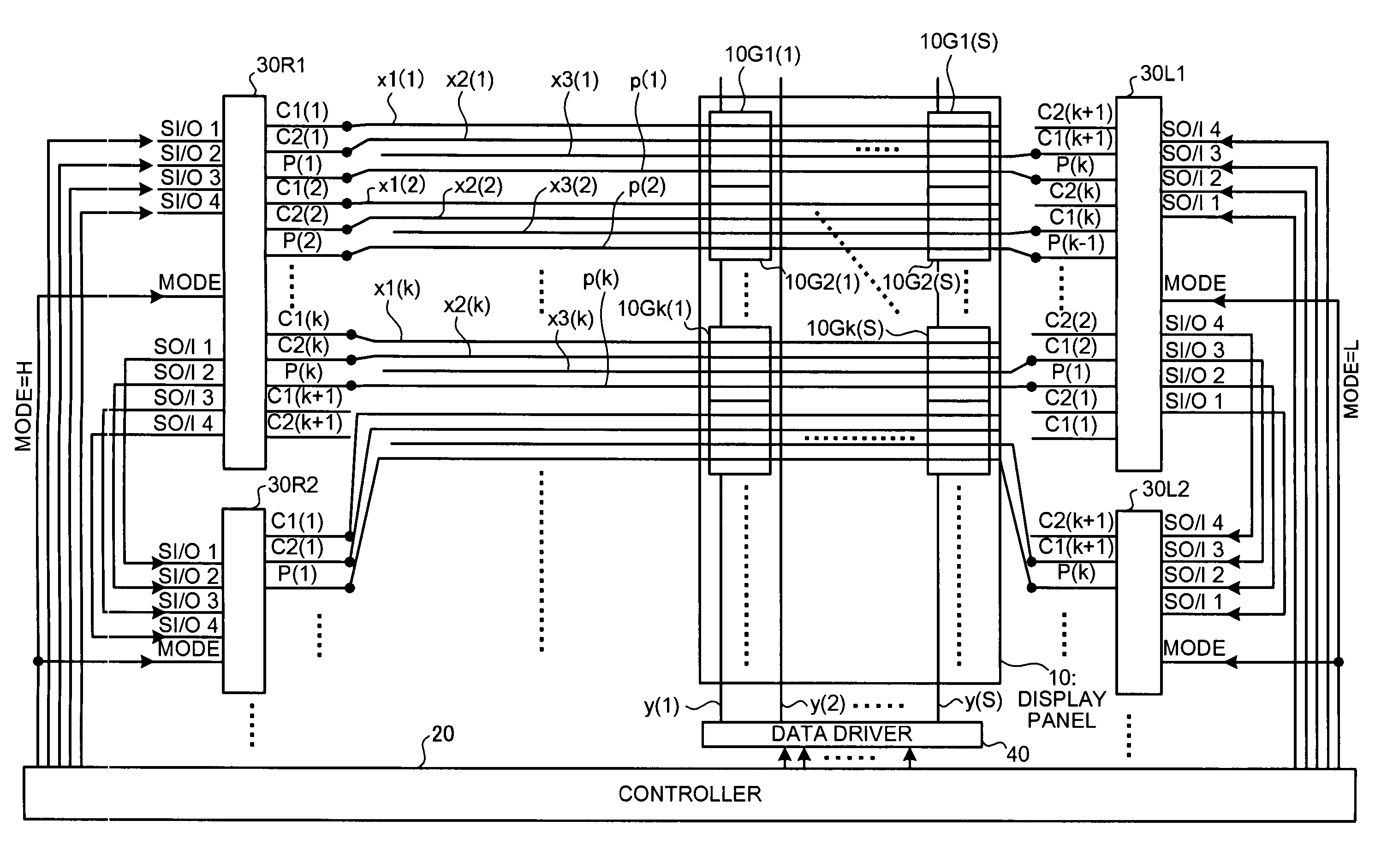
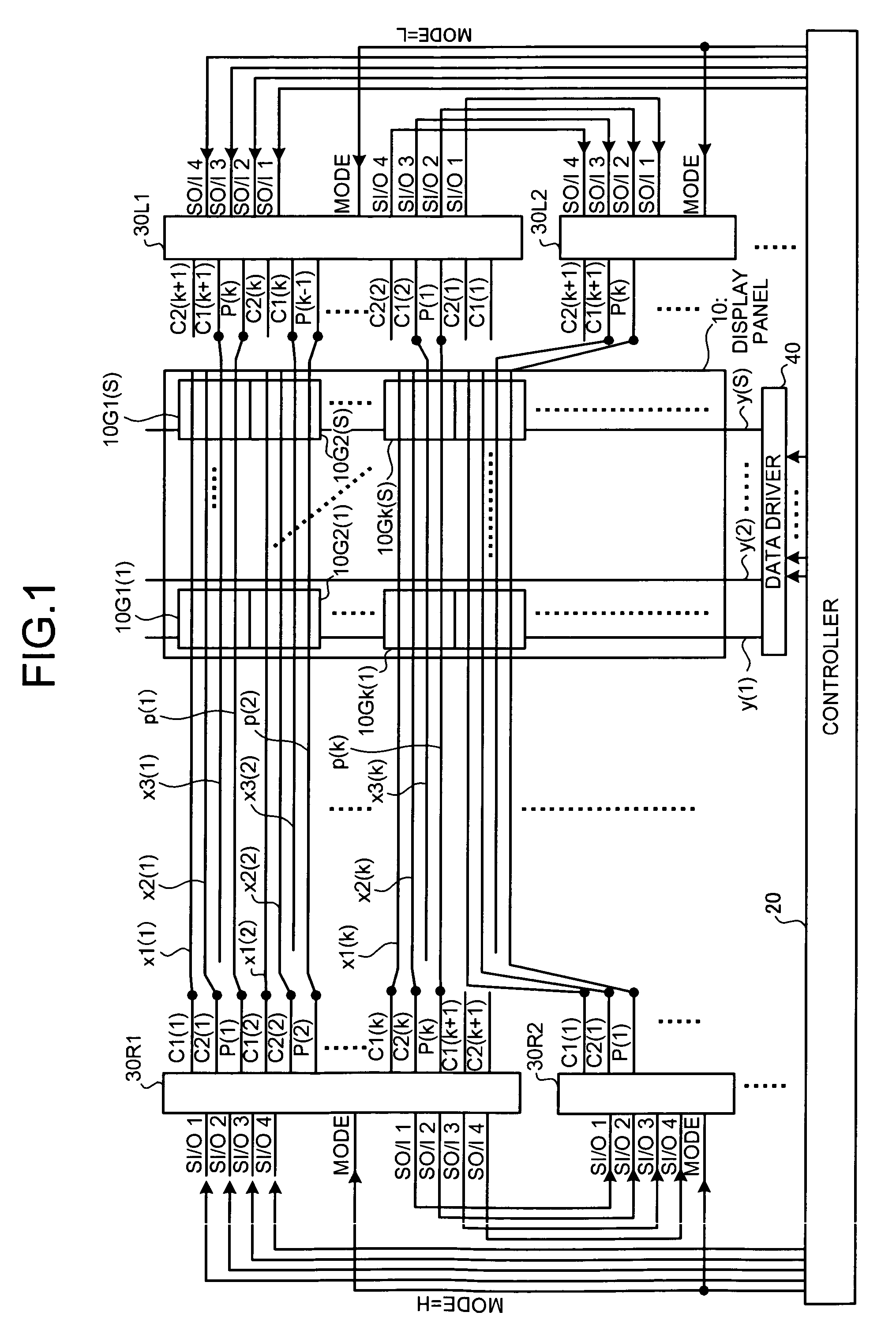
[0044]FIG. 1 is a block diagram of a structure of an image display apparatus according to the present invention. The image display apparatus shown in FIG. 1 includes a display panel 10, a controller 20, a gate drivers 30R1, a gate driver 30R2, . . . , a gate drier 30L1, a gate driver 30L2, . . . , and a data driver 40.

[0045]The display panel 10 includes a pixel circuit 10G1(1), . . . , a pixel circuit 10G1(s), a pixel circuit 10G2(1), . . . , a pixel circuit 10G2(s), a pixel circuit 10Gk(1), . . . , a pixel circuit 10Gk(s), . . . .

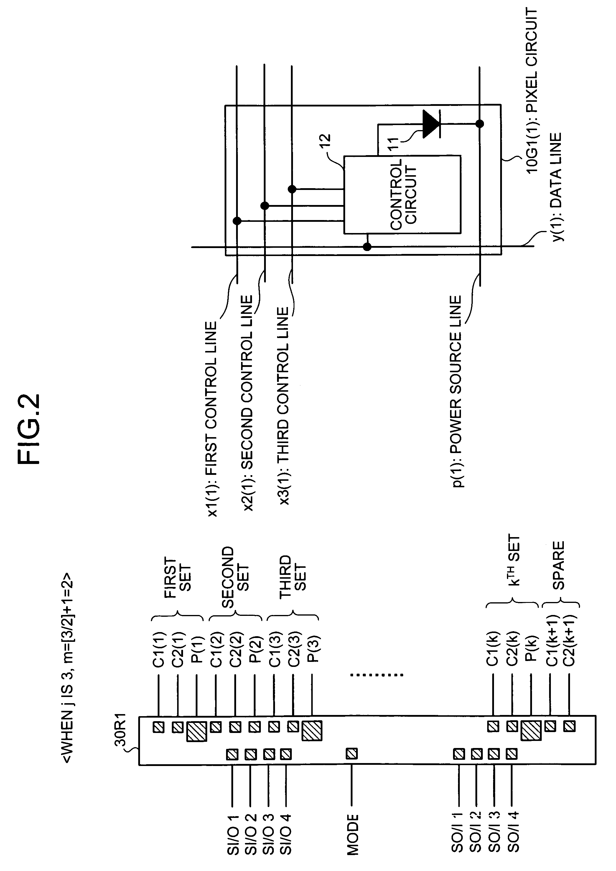
[0046]In the display panel 10, plural sets of four lines are arranged, one set for each row (provided in the horizontal direction in the drawing). For example, a first control line x1(1), a second control line x2(1), a third control line x3(1), and a power source line p(1) shown in FIG. 1 constitute one set.

[0047]Specifically, for a first row which corresponds to the pixel circuits 10G1(1) to 10G1(s) in the display panel, four lines, i.e., the first contro...

second embodiment

[0084]FIG. 6 is a diagram of a structure of the gate driver 50R1, the pixel circuit 10G1(1), or the like applied to the present invention. In FIG. 6, elements corresponding to the elements shown in FIG. 3 are denoted by the same reference characters.

[0085]In the pixel circuits 10G1(1)′ shown in FIG. 6, j first control lines x1(1), . . . , xj(1), and a first power source line p1(1) and a second power source line p2(1) are arranged in a row direction.

[0086]The gate driver 50R1 is provided with a plurality of pads, i.e., first to kth sets of pads. The first set includes a control pad C1(1), a control pad Cq(1), a control pad Cq+1(1), a control pad C1(1), a control pad C1+1(1), a control pad Cm(1), a power source pad P1(1), and a power source pad P2(1).

[0087]The second set includes a control pad C1(2), a control pad Cq(2), a control pad Cq+1(2), a control pad C1(2), a control pad C1+1(2), a control pad Cm(2), a power source pad P1(2), and a power source pad P2(2).

[0088]Similarly, the kt...


PUM


Abstract

A driver for driving a display panel having a light emitting element includes a plurality of control pads, each of which is electrically connected to a control line of the display panel; and a plurality of power source pads, each of which is electrically connected to a power source line of the display panel and is larger in area than the control pad. The control pads and the power source pads are arranged in line and an order of arrangement of the control pads and the power source pads is symmetrical with respect to a direction of pad arrangement.

Description

BACKGROUND OF THE INVENTION[0001]1. Field of the Invention[0002]The present invention relates to a driver for a display panel and an image display apparatus that employ an organic light-emitting diode (OLED), and more particularly to a driver for a display panel and an image display apparatus that can prevent generation of uneven luminance and allow space saving.[0003]2. Description of the Related Art[0004]Along with the growing popularity of mobile computing, demand for flat-type displays is increasing. Commonly used flat-type display is a liquid crystal display, which however is not immune to problems such as a narrow viewing angle and unfavorable response characteristics.[0005]In recent years, image displays employing OLEDs have attracted attentions as flat-type image displays with a wide viewing angle and good response characteristics. The OLED recombines positive holes and electrons injected into a light emitting layer to emit light.[0006]Such conventional image display apparat...

Claims


Application Information

Patent Timeline
Patent Type & Authority Patents(United States)
IPC IPC(8): G09G3/00G09G3/30G09G3/32H05B44/00
CPCG09G3/3233G09G3/3275G09G2300/0842G09G2300/0861G09G2310/0262G09G2320/0223G09G2320/0233
Inventor ONO, SHINYAKOBAYASHI, YOSHINAOMIWA, KOHICHI
Owner INNOLUX CORP
Why Eureka
Try Eureka