Chiplet display with electrode connectors

a chiplet display and electrode connector technology, applied in the field of electrode connector arrangement and connection of signal buss wires, can solve the problems of limited number of rows (or columns) of passive matrix drive devices, flicker can become perceptible, and currents necessary to drive an entire row (or column) of display, so as to improve pixel-driving performance and increase light-emitting area

Active Publication Date: 2013-12-03
GLOBAL OLED TECH
View PDF39 Cites 20 Cited by
  • Summary
  • Abstract
  • Description
  • Claims
  • Application Information

AI Technical Summary

Benefits of technology

[0019]The present invention provides a display having improved pixel-driving performance and increased light-emitting area.

Problems solved by technology

A passive-matrix drive device is also limited in the number of rows (or columns) that can be included in the device since the sequential nature of the row (or column) driving creates flicker.
If too many rows are included, the flicker can become perceptible.
Moreover, the currents necessary to drive an entire row (or column) in a display can be problematic since the power required for the non-imaging pre-charge and discharge steps of PM driving become dominant as the area of the PM display grows.
These problems limit the physical size of a passive-matrix display.
Thin-film transistors (TFTs) made from amorphous or polycrystalline silicon are relatively large and have lower performance compared to conventional transistors made in crystalline silicon wafers.
Moreover, such thin-film devices typically exhibit local or large-area non-uniformity across the glass substrate that results in non-uniformity in the electrical performance and visual appearance of displays employing such materials.
When employing an active-matrix control method for bottom—emitter light-emitting diode displays, the emissive area over the substrate is limited by the area required for the thin-film components or the crystalline silicon substrates.
It is preferred, however, to make the emissive area as large as possible, since the emissive area, especially for OLED devices, can limit display lifetime.
Since thin-film components, crystalline silicon substrates, and photo-lithographically formed control, power, and ground wires typically comprise opaque metal, such as aluminum, traditional display layout designs for bottom-emitter displays arrange the wires and thin-film components between the emissive areas so that emitted light is not obscured by the wires and thin-film components, which can otherwise absorb light and reduce device efficiency.
In these designs, the emissive area is limited by wires or thin-film components formed over the substrate, thereby reducing the lifetime of organic LED displays.

Method used


Image

  • Chiplet display with electrode connectors
  • Chiplet display with electrode connectors
  • Chiplet display with electrode connectors

Examples


Embodiment Construction

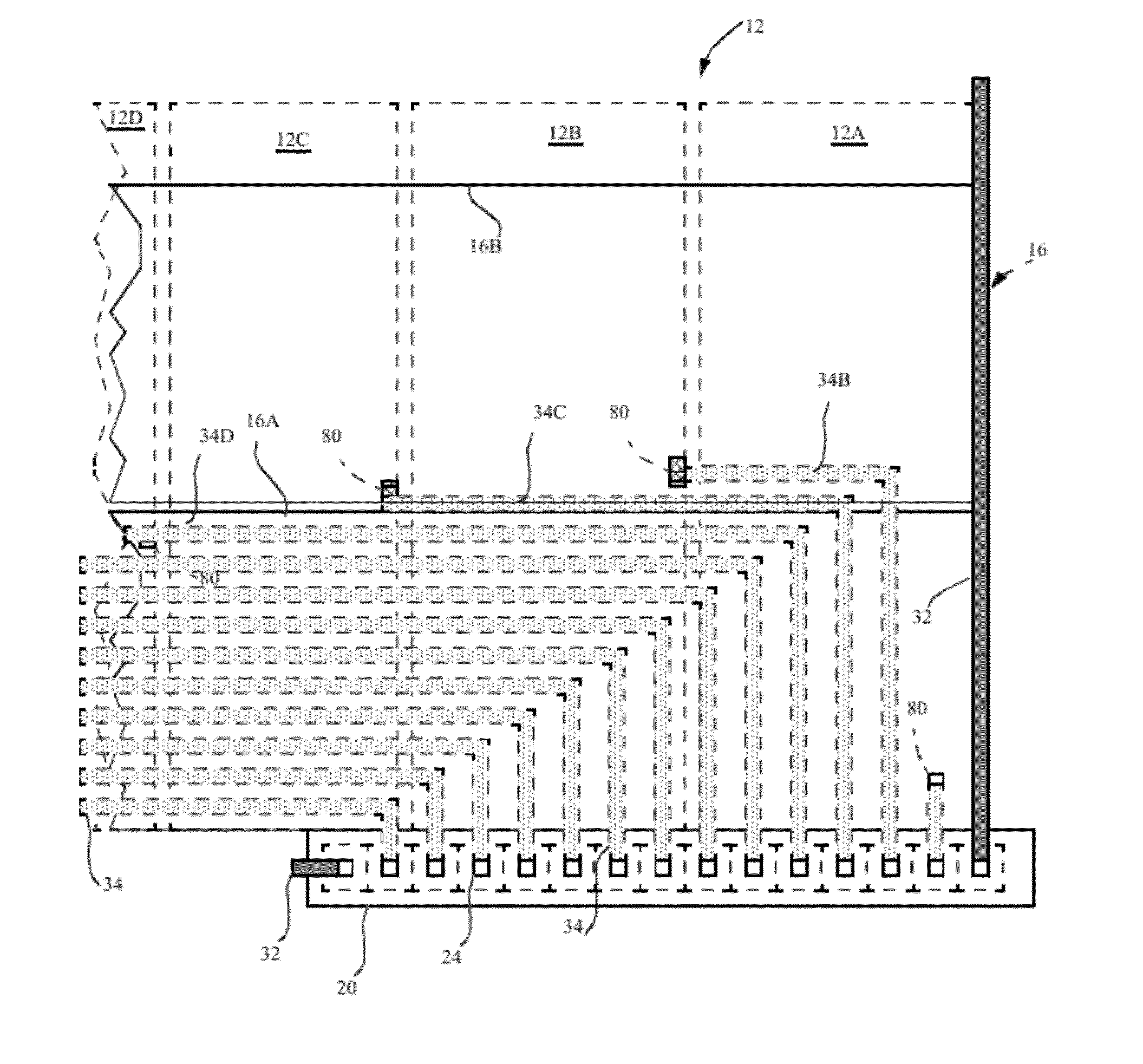
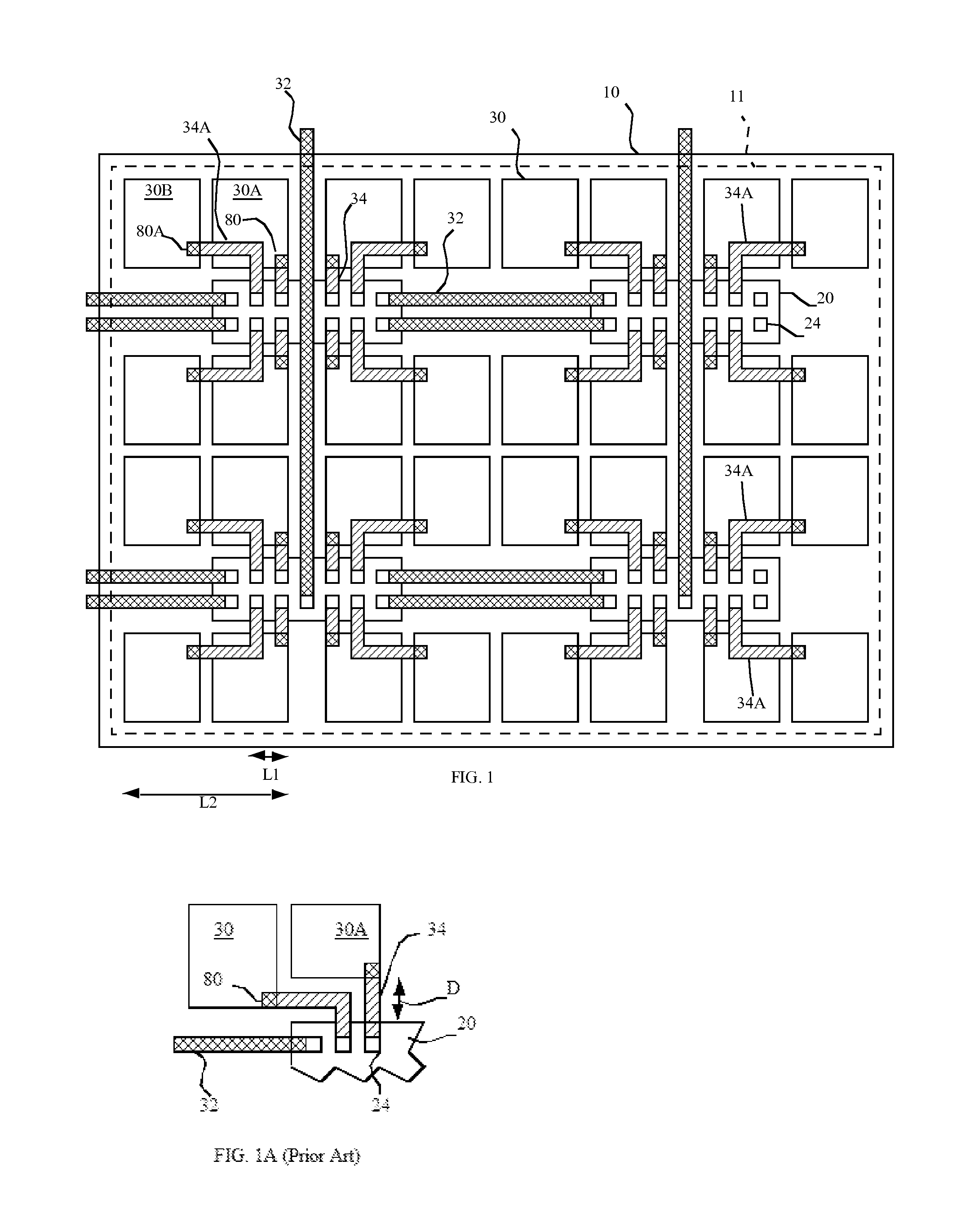
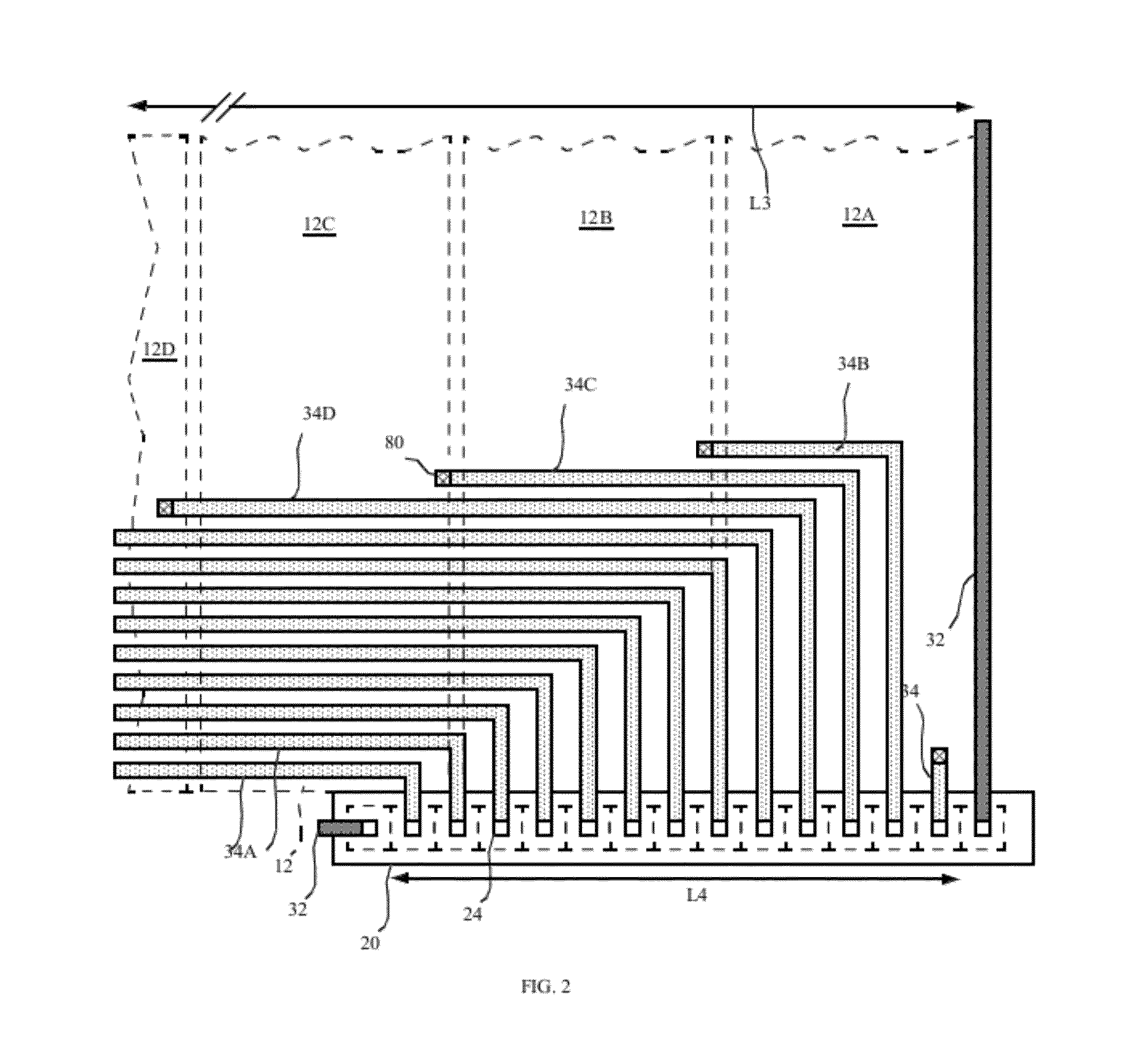
[0034]The present invention provides higher-performance pixel-driving circuits for driving pixels in an emissive display with increased light-emitting area. The higher-performance pixel-driving circuits are formed in chiplets having crystalline silicon substrates separate from the display substrate. Transistors formed in the crystalline silicon substrates are smaller and have higher performance than conventional thin-film transistors found in prior-art active-matrix displays. Because the transistors are smaller and located within chiplets, electrical connections from the pixel-driving circuitry to pixel electrodes are necessary and are more concentrated in a smaller area than the vias typically used in a TFT active-matrix circuit. Referring to FIGS. 1A and 9, in an example illustrating a chiplet design with a routing solution suggested by the prior art, a conventional routing scheme for the electrical connections to a chiplet would require a significant display substrate area for th...


PUM


Abstract

A display device comprising a transparent substrate, transparent electrodes, light-emitting layers, and reflective electrodes that define light-emitting pixels in which chiplets with pixel driving circuits are connected to pixel connection pads that are connected to the transparent electrode by an opaque electrode connector such that at least a portion of one opaque electrode connector overlaps at least a portion of a transparent electrode to which the opaque electrode connector is not electrically connected. The device provides a display having improved pixel-driving performance and increased light-emitting area.

Description

CROSS REFERENCE TO RELATED APPLICATIONS[0001]Reference is made to commonly-assigned, co-pending U.S. patent application Ser. No. 12 / 191,478, filed Aug. 14, 2008, entitled “OLED device with embedded chip driving” by Winters et al., commonly-assigned, co-pending U.S. patent application Ser. No. 12 / 191,462, filed Aug. 14, 2008, entitled “DISPLAY DEVICE WITH CHIPLETS” by Cok et al., commonly-assigned, co-filed U.S. patent application Ser. No. 12 / 272,043, filed Nov. 17, 2008 entitled “DISPLAY DEVICE WITH CHIPLETS AND HYBRID DRIVE” by Cok et al., commonly assigned, co-pending U.S. patent application Ser. No. 11 / 311,763, filed Dec. 19, 2005 entitled “OLED DEVICE HAVING IMPROVED POWER DISTRIBUTION’ by Cok; and commonly assigned co-pending U.S. patent application Ser. No. 12 / 369,163, filed Feb. 11, 2009, entitled “DISPLAY DEVICE WITH CHIPLETS AND LIGHT SHIELDS” by Cok et al.; the disclosures of which are incorporated by reference herein.FIELD OF THE INVENTION[0002]The present invention relat...

Claims


Application Information

Patent Timeline
Patent Type & Authority Patents(United States)
IPC IPC(8): G09G3/30
CPCH01L27/3255H01L27/3276H01L27/3288H01L51/5268H01L51/5284H10K59/129H10K59/179H10K59/131H10K50/854H10K50/865H10K59/00
Inventor COK, RONALD S.
Owner GLOBAL OLED TECH
Why Eureka
Try Eureka