Source/drain re-growth for manufacturing III-V based transistors

a technology of source/drain regrowth and transistors, which is applied in the direction of semiconductor devices, basic electric elements, electrical appliances, etc., can solve the problems of inability to achieve uniform etching depth d throughout the respective chip, difficulty in accurately controlling etching depth d, and inability to achieve uniform etching depth d. , to achieve the effect of improving short channel control, reducing external resistance of transistors, and increasing the drive current of transistors

Active Publication Date: 2013-12-31
TAIWAN SEMICON MFG CO LTD
View PDF95 Cites 0 Cited by
  • Summary
  • Abstract
  • Description
  • Claims
  • Application Information

AI Technical Summary

Benefits of technology

[0008]The advantageous features of the present invention include improved short channel control of III-V transistors and uniform threshold voltages for transistors throughout chips / wafers. Further, the external resistances of the transistors are reduced, and the drive currents of the transistors are increased.

Problems solved by technology

The above-described structure and process steps, however, suffer from process difficulties.
However, accurately controlling etching depth D is difficult.
Particularly, it is difficult to achieve uniform etching depth D throughout the respective chip.
However, distance Tins of the plurality of recesses at different locations of a chip / wafer may be different, resulting in non-uniformity in the performance of the resulting transistors.

Method used


Image

  • Source/drain re-growth for manufacturing III-V based transistors
  • Source/drain re-growth for manufacturing III-V based transistors
  • Source/drain re-growth for manufacturing III-V based transistors

Examples


Embodiment Construction

[0013]The making and using of the embodiments of the present invention are discussed in detail below. It should be appreciated, however, that the embodiments provide many applicable inventive concepts that can be embodied in a wide variety of specific contexts. The specific embodiments discussed are merely illustrative of specific ways to make and use the invention, and do not limit the scope of the invention.

[0014]Novel transistors comprising compound semiconductor materials of group III and group V elements (referred to as III-V compound semiconductors hereinafter) and the methods of forming the same are provided. The intermediate stages in the manufacturing of embodiments of the present invention are illustrated. The variations of the embodiments are discussed. Throughout the various views and illustrative embodiments of the present invention, like reference numbers are used to designate like elements.

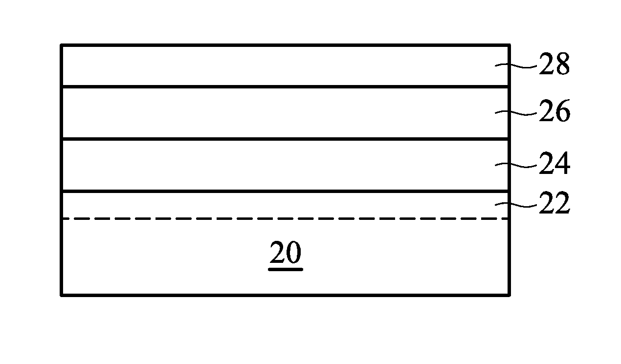
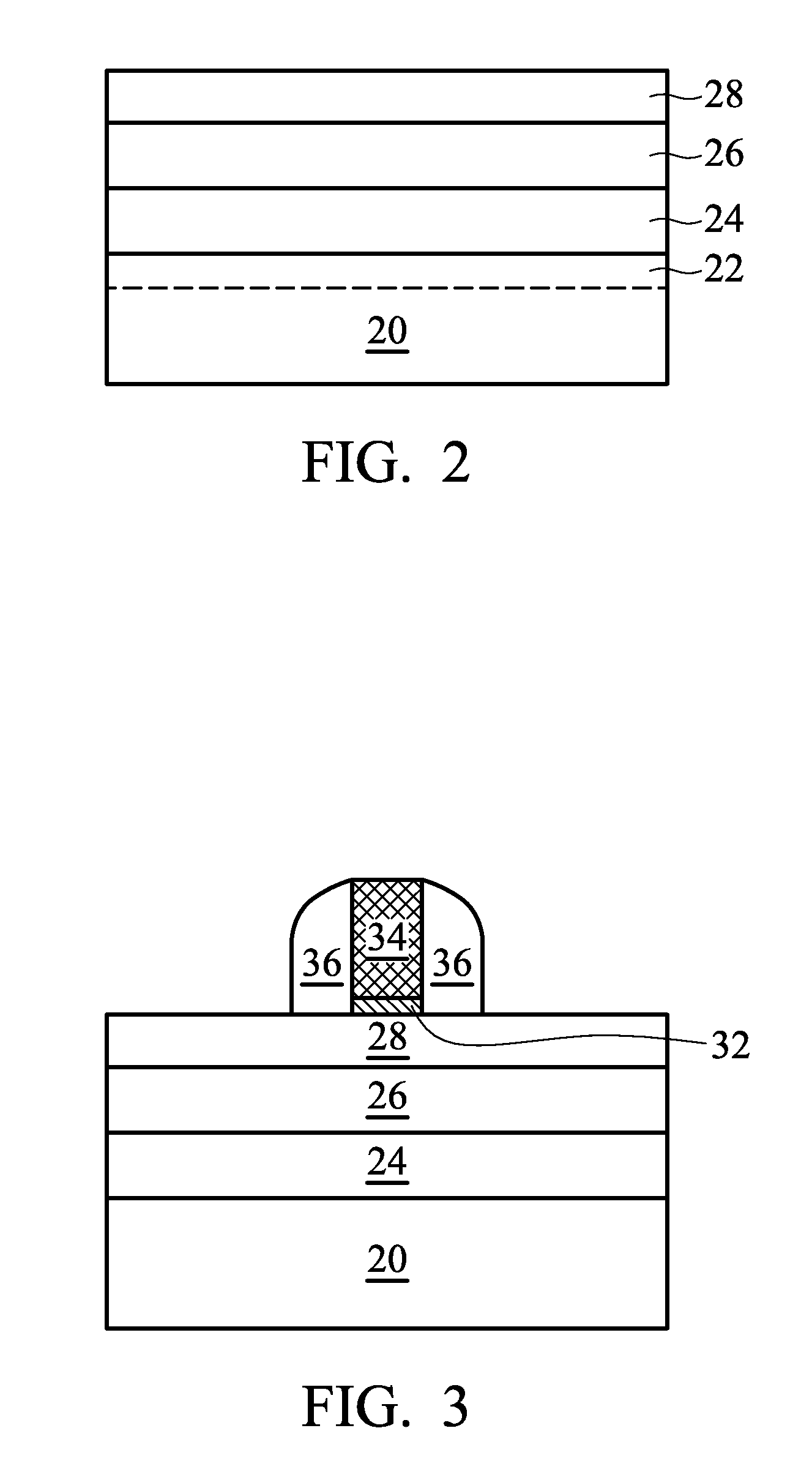
[0015]Referring to FIG. 2, substrate 20 is provided. Substrate 20 may be a semi...


PUM


Abstract

A method of forming an integrated circuit structure includes providing a substrate, and epitaxially growing a first semiconductor layer over the substrate. The first semiconductor layer includes a first III-V compound semiconductor material formed of group III and group V elements. The method further includes forming a gate structure on the first semiconductor layer, and forming a gate spacer on at least one sidewall of the gate structure. After the step of forming the gate structure, a second semiconductor layer including a second III-V compound semiconductor material is epitaxially grown on the first semiconductor layer.

Description

[0001]This application claims the benefit of U.S. Provisional Application No. 61 / 182,961 filed on Jun. 1, 2009, entitled “Source / Drain Re-Growth for Manufacturing III-V Based Transistors,” which application is hereby incorporated herein by reference.TECHNICAL FIELD[0002]This invention relates generally to integrated circuit structures, and more particularly to transistors comprising III-V compound semiconductors and methods for forming the same.BACKGROUND[0003]The speeds of metal-oxide-semiconductor (MOS) transistors are closely related to the drive currents of the MOS transistors, which drive currents are further closely related to the mobility of charges. For example, NMOS transistors have high drive currents when the electron mobility in their channel regions is high, while PMOS transistors have high drive currents when the hole mobility in their channel regions is high.[0004]Compound semiconductor materials of group III and group V elements (commonly known as III-V compound semi...

Claims


Application Information

Patent Timeline
Patent Type & Authority Patents(United States)
IPC IPC(8): H01L21/3205
CPCH01L29/66628H01L29/78H01L29/4236H01L29/66863H01L29/8128H01L29/66462H01L29/7783H01L21/28264
Inventor KO, CHIH-HSINWANN, CLEMENT HSINGJEN
Owner TAIWAN SEMICON MFG CO LTD
Why Eureka
Try Eureka