Process for producing substrate provided with metal pattern and substrate provided with metal laminate

a technology of metal pattern and substrate, which is applied in the manufacture of electric discharge tubes/lamps, instruments, and removal of conductive materials, etc., can solve the problems of difficult processing of metal film, small absorption of energy by metal film, and difficult to obtain high-output laser light in the ultraviolet ray region, etc., to achieve easy formation of desired metal patterns and facilitate processing of metal layers. , the effect of high accuracy

Inactive Publication Date: 2014-02-11
AGC INC
View PDF6 Cites 2 Cited by
  • Summary
  • Abstract
  • Description
  • Claims
  • Application Information

AI Technical Summary

Benefits of technology

[0013]Thus, the absorption amount of the laser light absorbed by the whole laminate is increased by using the assist layer which has a light absorptivity for the laser light different from that of the metal layer, which facilitates processing for forming the metal pattern.
[0043]According to the present invention, a substrate on which a metal pattern is formed with high accuracy can be produced.

Problems solved by technology

However, application of the processing method using a laser light described in patent document 1 or 2 as such to processing of a metal film involves a problem that processing of the metal film is difficult.
Specifically, there has been the problem that, although the region of laser beam which shows high thermal absorption efficiency for a metal film to be processed is an ultraviolet ray region, it is difficult to obtain a high-output laser light in the ultraviolet ray region.
On the other hand, when YAG layer of 1064 nm in wavelength is used in order to obtain a high laser output, absorption of energy by the metal film is so small that there has been involved a problem that processing is difficult unless the laser power is increased to a considerably high level.
For example, there has been the problem that, when the thickness of the metal film becomes 1 μm or more, processing thereof cannot be conducted with high accuracy even when the power of laser light is increased to 400 W or more.

Method used


Image

  • Process for producing substrate provided with metal pattern and substrate provided with metal laminate
  • Process for producing substrate provided with metal pattern and substrate provided with metal laminate
  • Process for producing substrate provided with metal pattern and substrate provided with metal laminate

Examples


embodiment 1

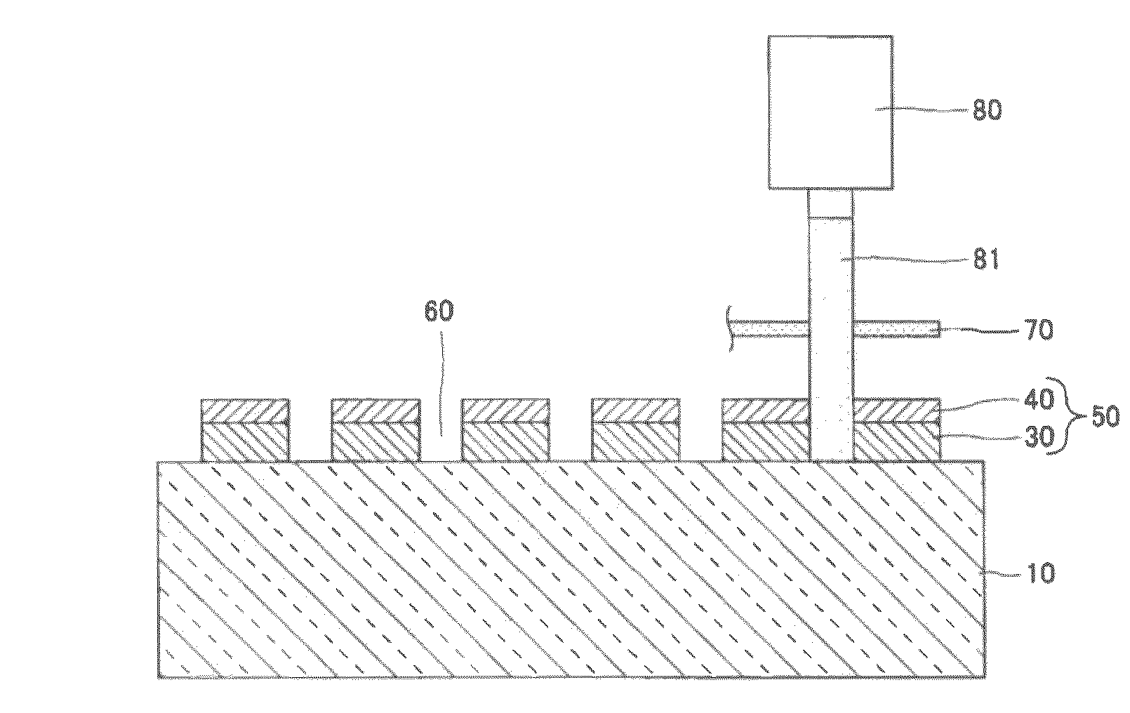
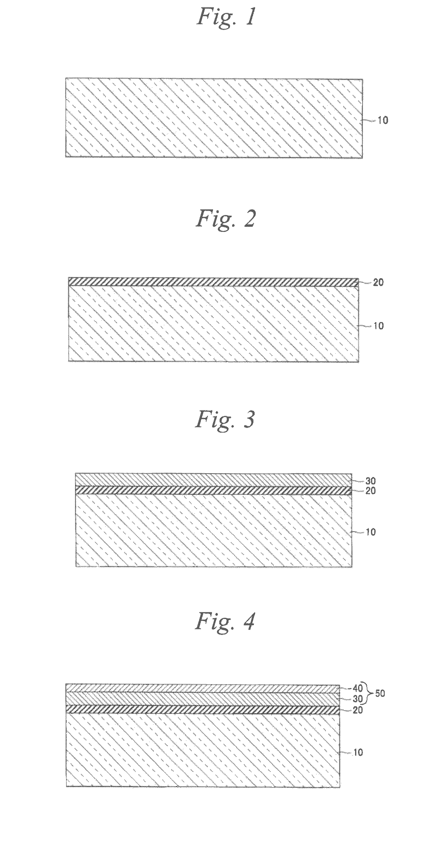
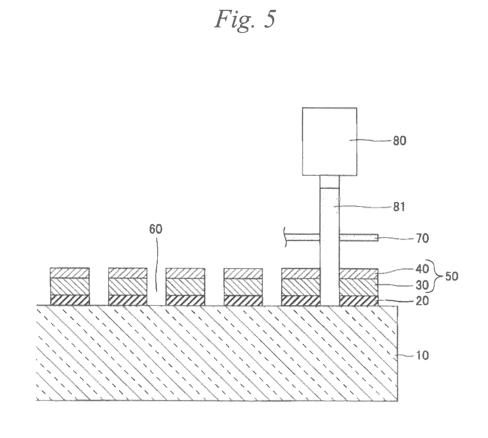
[0065]FIGS. 1 to 7 show one example of respective steps of the process for producing a substrate provided with a metal pattern in accordance with embodiment 1.

[0066]FIG. 1 shows one example of a step of preparing a substrate 10 in the process for producing a substrate provided with a metal pattern in accordance with this embodiment. In FIG. 1, a substrate 10 is shown to be prepared in a mounted state. As the substrate 10, substrates of various materials can be used. For example, a glass substrate 10 is preferably used. The glass substrate 10 is used in many cases as a display panel material of a flat panel display such as a plasma display panel or a liquid crystal panel. In this embodiment, description is made by reference to an example in which a glass substrate is used as the substrate 10. However, various substrates 10 may be used as long as they have resistance to heat to be generated upon laser processing and to laser irradiation thereupon.

[0067]FIG. 2 shows one example of a lo...

embodiment 2

[0106]FIGS. 10 to 14 show one example of the process for producing a substrate provided with a metal pattern in accordance with embodiment 2.

[0107]FIG. 10 shows one example of a step of preparing the substrate 10 in the process for producing the substrate provided with a metal pattern in accordance with embodiment 2. Since the step shown in FIG. 10 is the same as that described with respect to FIG. 1 for embodiment 1, the same reference numbers are given, with descriptions thereon being omitted.

[0108]FIG. 11 shows one example of a metal layer-forming step in the process for producing a substrate provided with a metal pattern in accordance with embodiment 2. In the metal layer-forming step, a metal layer 30 is formed on the substrate 10. In embodiment 1, the low-reflective layer 20 is formed on the substrate 10 whereas, in the process for producing a substrate provided with a metal pattern in accordance with embodiment 2, the low-reflective layer 20 is not formed but the metal layer ...

example 1

[0121]Item (a) in FIG. 15 shows the results of Example 1. In Example 1, a metal layer 30 of copper (Cu) was formed on a substrate 10 for plasma display (PD), and laser processing was conducted. The thickness of the copper metal layer 30 was 2,000 Å. It is seen that, even when a laser light of 74 W in power and 1.2 J / cm2 in fluence was irradiated, the single metal layer 30 composed of Cu was not removed at all though the thickness of the layer was comparatively as thin as 2,000 Å, thus no metal pattern being formed.


PUM

PropertyMeasurementUnit
thicknessaaaaaaaaaa
wavelengthaaaaaaaaaa
thicknessaaaaaaaaaa

Abstract

The present invention relates to a process for producing a substrate provided with a metal pattern by forming a pattern of a metal layer on a substrate using a laser light, the process including: a step of preparing a substrate in which the metal layer is formed on a surface thereof; a step of forming on the metal layer an assist layer which comprises a metal material different from that of the metal layer and which has a light absorptivity for the laser light different from that of the metal layer, thereby forming a metal laminate on the substrate; and a step of patterning the metal layer by irradiating the metal laminate with the laser light to remove a laser light-irradiated portion of the metal laminate, thereby forming a metal pattern on the substrate.

Description

FIELD OF THE INVENTION[0001]The present invention relates to a process for producing a substrate provided with a metal pattern, in which a metal pattern is formed by using a laser light, and relates to a substrate provided with a metal laminate.BACKGROUND OF THE INVENTION[0002]As a process for producing display panel for flat panel display such as plasma display panel, there has been known a technique of providing a thin film for a transparent electrode on a glass substrate, and irradiating the thin film for transparent electrode with a laser beam to conduct patterning, thus forming a transparent electrode (see, for example, patent documents 1 and 2). According to such processing method utilizing laser beam, the number of production steps can be decreased in comparison with the photo lithography steps and, further, necessity of preparing a large-sized photo mask is eliminated. Still further, the production line is made more compact, which serves to reduce the land area necessary for...

Claims


Application Information

Patent Timeline
Patent Type & Authority Patents(United States)
IPC IPC(8): H01J11/34H05K3/08H01J11/22B23K26/00H01J9/02H05K3/00
CPCB23K26/0048B23K26/409B23K26/365B23K26/0006B23K26/40B23K26/361B23K2103/172H01J9/02H01J17/04H01J17/49
Inventor NIU, GUANGYAO
Owner AGC INC
Why Eureka
Try Eureka