
Wired circuit board

a wired circuit board and wire technology, applied in the direction of printed circuits, printed circuit details, circuit susbtrate materials, etc., can solve the problems of unstable impedance in the wiring portion, degrade the accuracy, etc., and achieve the effect of reliably stabilizing the impedance and improving the placement accuracy of the second wir

Inactive Publication Date: 2014-03-04
NITTO DENKO CORP
View PDF27 Cites 10 Cited by
  • Summary
  • Abstract
  • Description
  • Claims
  • Application Information

AI Technical Summary

Benefits of technology

[0009]An object of the present invention is to provide a wired circuit board which is excellent in the accuracy of placement of the second wire and allows stabilization of impedance in a first wire and a second wire.
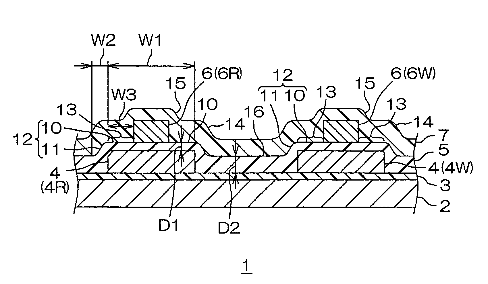
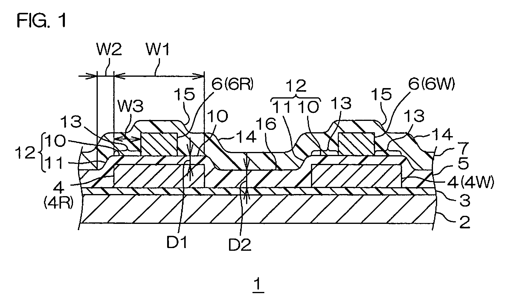
[0012]In the wired circuit board according to the present invention, even when a stepped portion is formed in the second insulating layer covering the first wire, since the width of the second wire is smaller than that of the first wire, the second wire is formed on a flat portion of the second insulating layer inside the stepped portion. This allows an improvement in the accuracy of placement of the second wire. As a result, it is possible to reliably stabilize the impedance of each of the first wire and the second wire.

Problems solved by technology

When each of the first conductor for writing and the first conductor for reading is formed on the first insulating layer formed with such stepped portions to have the same width as that of each of the second conductor for reading and the second conductor for writing, displacement of the first conductor for writing and the first conductor for reading may occur due to the stepped portions to degrade the accuracy of placement.
As a result, there is a problem that impedance in the wiring portion becomes unstable.

Method used


Image

  • Wired circuit board
  • Wired circuit board
  • Wired circuit board

Examples


example 1

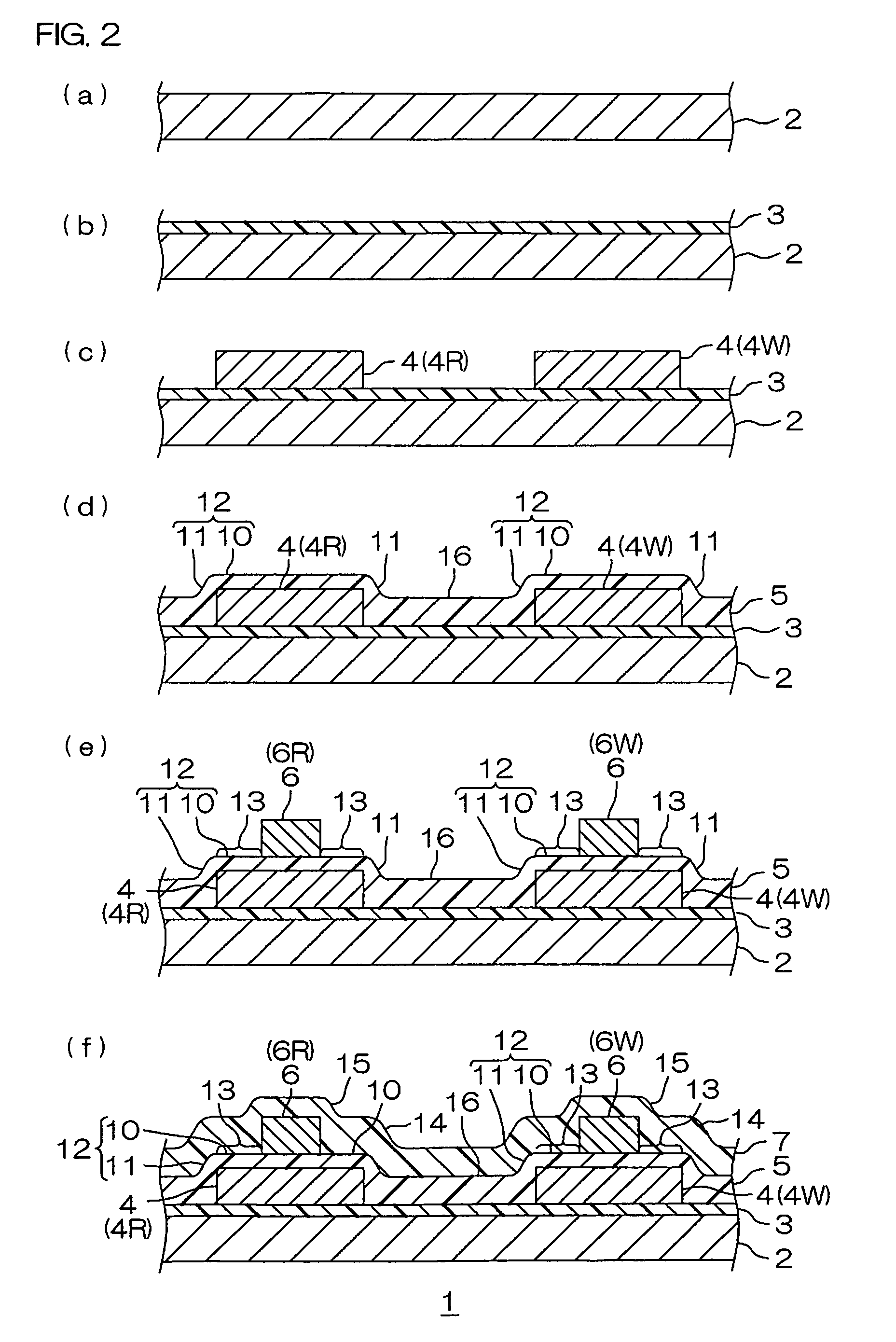
[0075]First, a metal supporting board made of a stainless steel foil (SUS304) having a thickness of 25 μm was prepared (see FIG. 2(a)). Then, a varnish of a photosensitive polyamic acid resin was coated on the entire upper surface of the metal supporting board, dried, exposed to light after drying, developed, and further cured by heating to form an insulating base layer made of polyimide having a thickness of 10 μm (see FIG. 2(b)).

[0076]Subsequently, first wires and first terminal portions were formed by an additive method on the insulating base layer.

[0077]In the additive method, a chromium thin film having a thickness of 0.03 μm and a copper thin film having a thickness of 0.07 μm were successively formed, each as a first metal thin film, by chromium sputtering and copper sputtering on the entire upper surface of the insulating base layer. Then, a plating resist in a pattern reverse to the pattern of the first wires and the first terminal portions was formed on the surface of the ...


PUM


Abstract

A wired circuit board includes a first insulating layer, a first wire formed on the first insulating layer, a second insulating layer formed on the first insulating layer so as to cover the first wire, and a second wire placed opposite to the first wire in a thickness direction and formed in a smaller width than that of the first wire.

Description

CROSS-REFERENCE TO RELATED APPLICATIONS[0001]This patent application claims the benefit of U.S. Provisional Application No. 60 / 960,981, filed on Oct. 24, 2007, and claims priority from Japanese Patent Application No. 2007-268292, filed on Oct. 15, 2007, the contents of which are herein incorporated by reference in their entirety.BACKGROUND OF THE INVENTION[0002]1. Field of the Invention[0003]The present invention relates to a wired circuit board and, more particularly, to a wired circuit board such as a suspension board with circuit or a flexible wired circuit board.[0004]2. Description of Related Art[0005]A wired circuit board such as a suspension board with circuit or a flexible wired circuit board includes, e.g., an insulating base layer, a conductive layer formed on the insulating base layer and including a plurality of wires, and an insulating cover layer formed on the insulating base layer and covering the conductive layer.[0006]For example, to stabilize the impedance of the c...

Claims


Application Information

Patent Timeline
Patent Type & Authority Patents(United States)
IPC IPC(8): H05K1/03H05K1/00
CPCH05K1/056H05K3/4644H05K1/0248H05K2201/09845H05K2201/09672H05K1/0245H05K3/44
Inventor KAMEI, KATSUTOSHIOHSAWA, TETSUYAHO, VOON YEE
Owner NITTO DENKO CORP
Learn More