Display device and method of driving the same

a display device and drive circuit technology, applied in the field of current-driven display devices, can solve the problems of difficult design of pixel circuits and drive circuits, difficult suppression, and easy fluctuation of luminance and voltage between the luminance and voltage of organic el elements, and achieve the effect of reducing the potential of the control terminal of the drive elemen

Active Publication Date: 2014-03-18
SHARP KK
View PDF35 Cites 4 Cited by
  • Summary
  • Abstract
  • Description
  • Claims
  • Application Information

AI Technical Summary

Benefits of technology

[0043]According to the first or eleventh aspect of the present invention, by controlling the compensation switching element to a conducting state, the drive element is placed in a state in which the threshold voltage is applied to the control terminal thereof. Thereafter, by switching the potential provided to the second electrode of the compensation capacitor to another with the compensation switching element maintaining the conducting state, a write potential according to display data and the threshold voltage is provided to the control terminal of the drive element. Except for the case of black display, the drive element is placed in a conducting state and thus a current according to the mobility of the drive element flows through the compensation switching element and the drive element, and the potential at the control terminal of the drive element changes according to the mobility of the drive element. By this, upon light emission of the electro-optic element, a current that is not affected by variations in the threshold voltage of the drive element nor by variations in the mobility of the drive element is allowed to flow through the electro-optic element. Accordingly, both variations in the threshold voltage of the drive element and variations in the mobility of the drive element can be compensated for, and thus the electro-optic element is allowed to emit light at a desired luminance.
[0044]According to the second aspect of the present invention, in a display device including pixel circuits, each including an electro-optic element, a drive element, three switching elements (for compensation, writing, and interruption), and two capacitors (for compensation and holding), a current that is not affected by variations in the threshold voltage of the drive element nor by variations in the mobility of the drive element is allowed to flow through the electro-optic element, whereby both variations in the threshold voltage of the drive element and variations in the mobility of the drive element can be compensated for.
[0045]According to the third or twelfth aspect of the present invention, by controlling the writing switching element and the compensation switching element to a conducting state and controlling the interruption switching element to a non-conducting state while providing a reference potential to the data line, a potential where variations in the threshold voltage of the drive element are corrected can be provided to the control terminal of the drive element. Then, by switching the potential provided to the second electrode of the compensation capacitor to another with the states of the respective switching elements being maintained, a write potential according to display data and the threshold voltage can be provided to the control terminal of the drive element. Thereafter, the potential at the control terminal of the drive element changes according to the mobility of the drive element. By this, a current that is not affected by variations in the threshold voltage of the drive element nor by variations in the mobility of the drive element is allowed to flow through the electro-optic element, whereby both variations in the threshold voltage of the drive element and variations in the mobility of the drive element can be compensated for.
[0046]According to the fourth aspect of the present invention, in a display device including pixel circuits, each including an electro-optic element, a drive element, three switching elements (for compensation, writing, and interruption), and a compensation capacitor, a current that is not affected by variations in the threshold voltage of the drive element nor by variations in the mobility of the drive element is allowed to flow through the electro-optic element, whereby both variations in the threshold voltage of the drive element and variations in the mobility of the drive element can be compensated for.
[0047]According to the fifth or thirteenth aspect of the present invention, by controlling the writing switching element and the compensation switching element to a conducting state and controlling the interruption switching element to a non-conducting state while providing a data potential to the data line, a potential where variations in the threshold voltage of the drive element are corrected can be provided to the control terminal of the drive element. Then, by switching the potential provided to the control wiring line connected to the second electrode of the compensation capacitor to a suitable level with the states of the respective switching elements being maintained, a write potential according to display data and the threshold voltage can be provided to the control terminal of the drive element. Thereafter, the potential at the control terminal of the drive element changes according to the mobility of the drive element. By this, a current that is not affected by variations in the threshold voltage of the drive element nor by variations in the mobility of the drive element is allowed to flow through the electro-optic element, whereby both variations in the threshold voltage of the drive element and variations in the mobility of the drive element can be compensated for.
[0048]According to the sixth aspect of the present invention, by providing, to the data line, a reference potential that is closer to the potential at the control terminal of the drive element than the data potential, the change in potential at the control terminal of the drive element can be reduced. Accordingly, even if the mobility of the drive element is high, the influence of the mobility of the drive element exerted on the potential at the control terminal of the drive element can be reduced, and thus both variations in the threshold voltage of the drive element and variations in the mobility of the drive element can be compensated for.

Problems solved by technology

However, the relationship between the luminance and voltage of the organic EL elements easily fluctuates by the influence of drive time, ambient temperature, etc.
Due to this, when a voltage control type drive scheme is applied to the organic EL display, it is very difficult to suppress, variations in the luminance of the organic EL elements.
The current program scheme, however, has the following problems.
First, since a very small amount of current is handled, it is difficult to design pixel circuits and drive circuits.
Second, since the influence of parasitic capacitance is likely to be received while a current signal is set, it is difficult to achieve an increase in area.

Method used


Image

  • Display device and method of driving the same
  • Display device and method of driving the same
  • Display device and method of driving the same

Examples


first embodiment

[0077](First Embodiment)

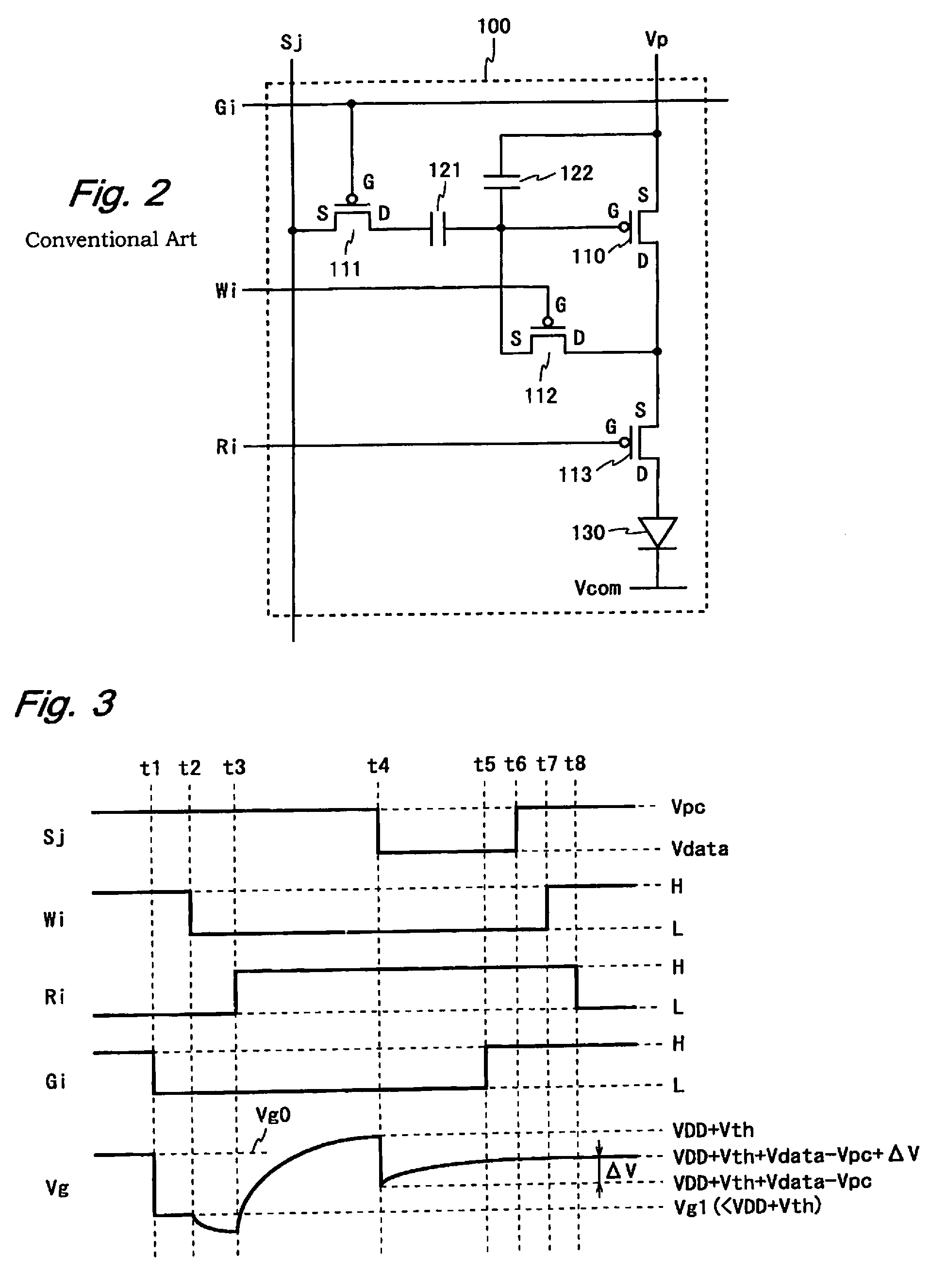
[0078]FIG. 2 is a circuit diagram of a pixel circuit included in a display device according to the first embodiment of the present invention. A pixel circuit 100 shown in FIG. 2 includes a driving TFT 110, switching TFTs 111 to 113, capacitors 121 and 122, and an organic EL element 130. All of the TFTs included in the pixel circuit 100 are of a p-channel type. The pixel circuit 100 is also described in Patent Document 1 (International Publication Pamphlet No. WO 98 / 48403).

[0079]The pixel circuit 100 is connected to a power supply wiring line Vp, a common cathode Vcom, a scanning line Gi, control wiring lines Wi and Ri, and a data line Sj. Of them, to the power supply wiring line Vp and the common cathode Vcom are respectively applied fixed potentials VDD and VSS (note that VDD>VSS). The common cathode Vcom is a cathode common to all organic EL elements 130 in the display device.

[0080]Terminals of the TFTs denoted as G, S, and D in FIG. 2 are referred to as a ...

second embodiment

[0102](Second Embodiment)

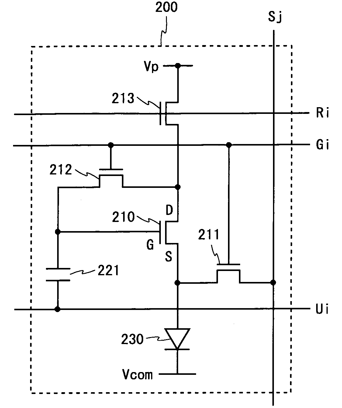
[0103]FIG. 5 is a circuit diagram of a pixel circuit included in a display device according to the second embodiment of the present invention. A pixel circuit 200 shown in FIG. 5 includes a driving TFT 210, switching TFTs 211 to 213, a capacitor 221, and an organic EL element 230. All of the TFTs included in the pixel circuit 200 are of an n-channel type. The pixel circuit 200 is also described in another application (Japanese Patent Application No. 2008-131568) having a common applicant and a common inventor with the present application.

[0104]The pixel circuit 200 is connected to a power supply wiring line Vp, a common cathode Vcom, a scanning line Gi, control wiring lines Ri and Ui, and a data line Sj. Of them, to the power supply wiring line Vp and the common cathode Vcom are respectively applied fixed potentials VDD and VSS (note that VDD>VSS). The common cathode Vcom is a cathode common to all organic EL elements 230 in the display device.

[0105]In the p...

third embodiment

[0130](Third Embodiment)

[0131]A display device according to the third embodiment of the present invention includes a pixel circuit 200 shown in FIG. 5, as does a display device according to the second embodiment. The display device according to the present embodiment drives the pixel circuit 200 according to a timing chart (FIG. 9) different from that in the second embodiment.

[0132]FIG. 9 is a timing chart showing a method of driving the pixel circuit 200 in the display device according to the present embodiment. As shown in FIG. 9, in the display device according to the present embodiment, during the period from time t4 to time t5 (mobility compensation period), the potential of a data line Sj is a reference potential Vpc which is higher than a data potential Vdata. Except for this point, the timing chart shown in FIG. 9 is the same as that shown in FIG. 6.

[0133]As such, in the display device according to the present embodiment, after the potential of a control wiring line Ui is ch...


PUM


Abstract

Switching TFTs are controlled to a conducting state and a switching TFT to a non-conducting state, to provide a potential according to a threshold voltage to a gate terminal of a driving TFT. Then, in at least one embodiment, with the TFT maintaining the conducting state, a potential of a data line Sj is changed from a reference potential Vpc to a data potential Vdata to place the TFT in a conducting state. At this time, a current Ia flows and thus the gate terminal potential of the TFT rises. The higher the mobility of the TFT, the larger the amount of change in gate terminal potential and the smaller the current flowing through an organic EL element upon light emission. By this, a current that is not affected by variations in the threshold voltage of the TFT nor by variations in the mobility of the TFT flows through the organic EL element. Thus, in a current-driven type display device, variations in both the threshold voltage and mobility of a drive element are compensated for.

Description

TECHNICAL FIELD[0001]The present invention relates to a display device, and more particularly, to a current-driven type display device such as an organic EL display or an FED, and a method of driving the display device.BACKGROUND ART[0002]In recent years, there has been an increasing demand for thin, lightweight, and fast response display devices. Correspondingly, research and development for organic EL (Electro Luminescence) displays and FEDs (Field Emission Displays) have been actively conducted.[0003]Organic EL elements included in an organic EL display emit light at higher luminance with a higher voltage applied thereto and a larger amount of current flowing therethrough. However, the relationship between the luminance and voltage of the organic EL elements easily fluctuates by the influence of drive time, ambient temperature, etc. Due to this, when a voltage control type drive scheme is applied to the organic EL display, it is very difficult to suppress, variations in the lumin...

Claims


Application Information

Patent Timeline
Patent Type & Authority Patents(United States)
IPC IPC(8): G09G3/32
CPCG09G2310/0262G09G3/3233G09G2300/0861G09G2300/0852G09G2320/045G09G2320/043G09G3/3291G09G3/3266G09G2300/0842G09G2300/0819
Inventor OHHASHI, SEIJI
Owner SHARP KK
Why Eureka
Try Eureka