
Continuous clocking mode for TDI binning operation of CCD image sensor

a ccd image sensor and continuous clocking technology, applied in the field device operation, can solve the problems of reducing the ability of ccd image sensor in tdi mode, not being completely eliminated, and artifacts becoming even larger and deeper

Active Publication Date: 2014-04-08
TELEDYNE DIGITAL IMAGING INC
View PDF3 Cites 9 Cited by
  • Summary
  • Abstract
  • Description
  • Claims
  • Application Information

AI Technical Summary

Benefits of technology

The continuous clocking technique significantly reduces artifacts and enhances the modulation transfer function, improving the CCD image sensor's ability to resolve high spatial frequencies and maintain signal strength even with higher binning factors.

Problems solved by technology

This results in artifacts associated with mapping the analog movement of the object onto a discrete set of elements of the CCD array in a TDI imaging mode.
Artifacts that are associated with the discrete movement of the charge in the CCD image sensor during TDI operation are inherent to the TDI modality and can not be completely eliminated.
This results in reduced ability of CCD image sensor in TDI mode to resolve high spatial frequencies in the scanning direction.
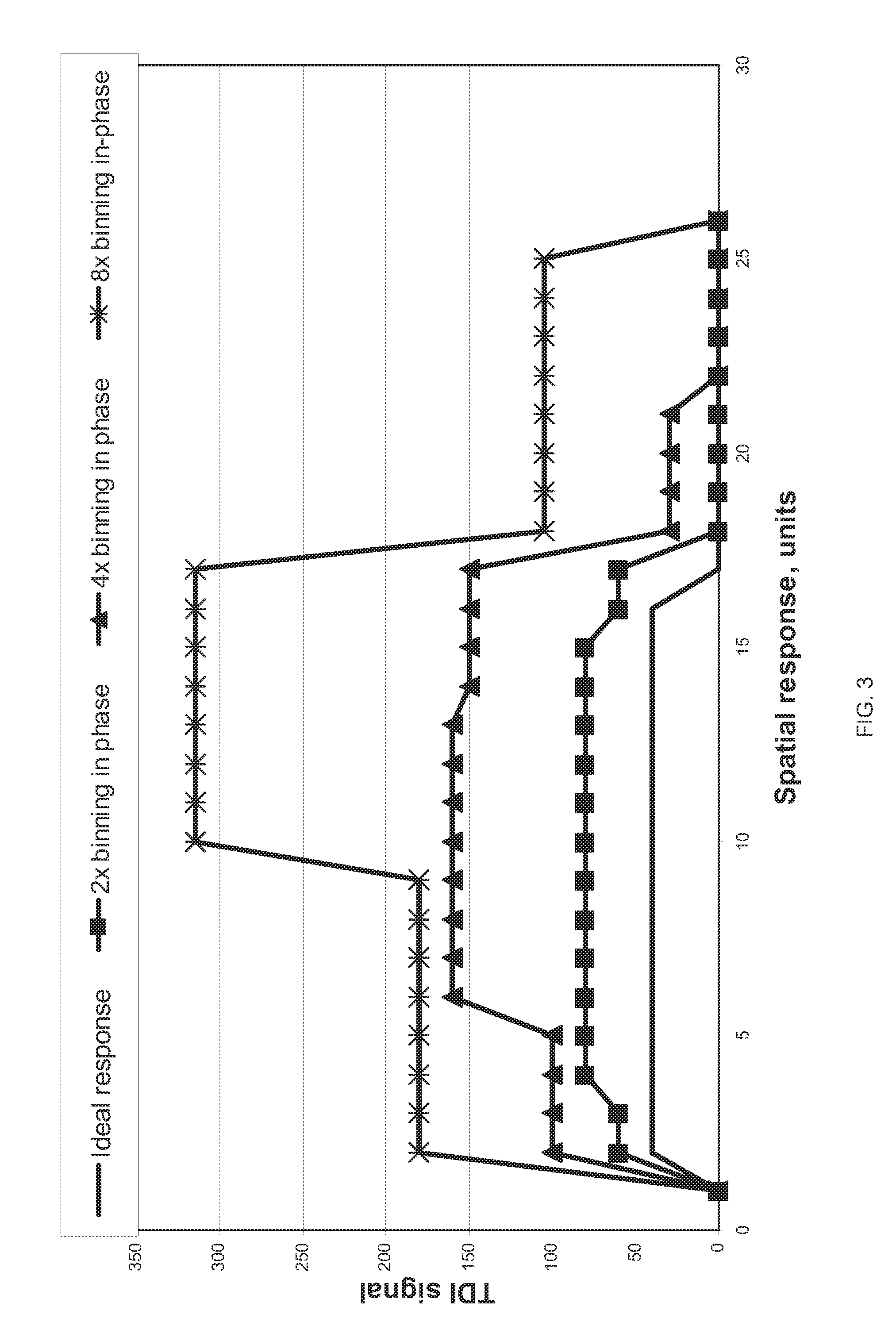
These artifacts become even larger and more profound if an additional increase of sensitivity is achieved by binning the CCD image sensor array in the direction of the charge movement.
TDI operation with binning results in significant mismatch between shifting the charge packets within the CCD image sensor and the continuous speed of mechanical scanning.

Method used


Image

  • Continuous clocking mode for TDI binning operation of CCD image sensor
  • Continuous clocking mode for TDI binning operation of CCD image sensor
  • Continuous clocking mode for TDI binning operation of CCD image sensor

Examples


Embodiment Construction

[0016]It will be appreciated that for simplicity and clarity of illustration, where considered appropriate, numerous specific details are set forth in order to provide a thorough understanding of the exemplary embodiments described herein. However, it will be understood by those of ordinary skill in the art that the embodiments described herein may be practiced without these specific details. In other instances, well-known methods, procedures and components have not been described in detail so as not to obscure the embodiments described herein. Furthermore, this description is not to be considered as limiting the scope of the embodiments described herein in any way, but rather as merely describing the implementations of various embodiments.

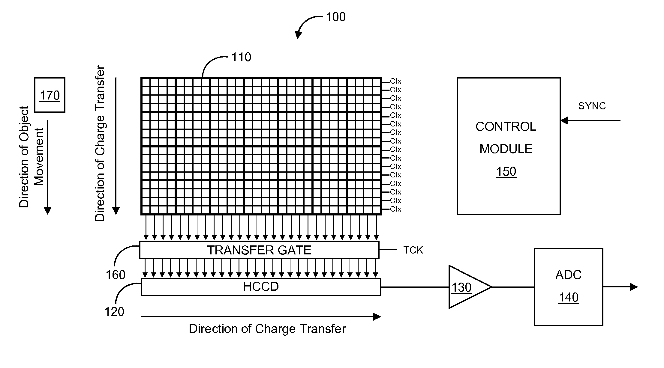
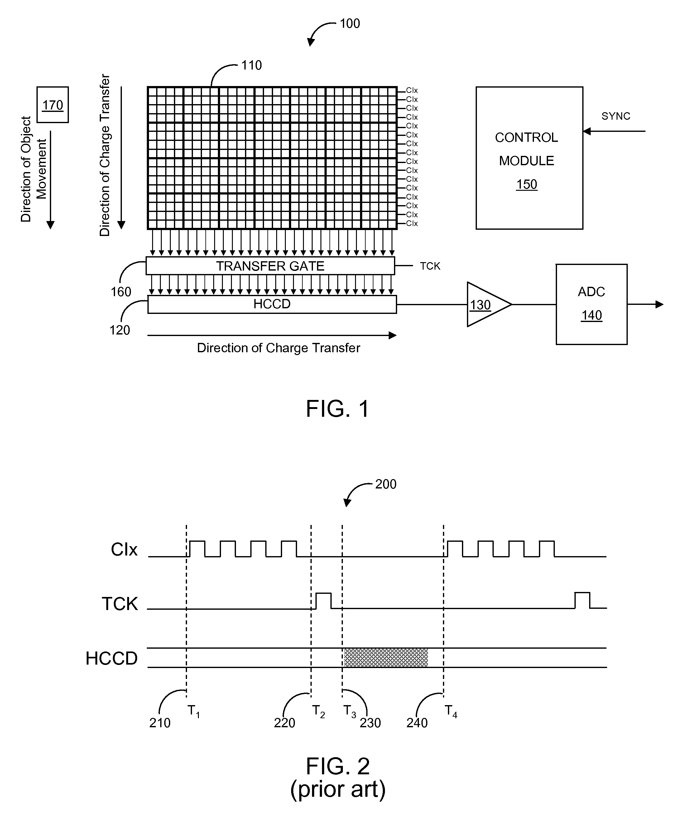
[0017]Reference is first made to FIG. 1, shown is a block diagram of an embodiment of a CCD image sensor 100 for illustrating time delay and integration technology and binning. CCD image sensor 100 consists of array 110 of photosensitive charge-co...


PUM


Abstract

A device and method for continuous vertical clocking a charge-coupled device image sensor operating in a time delay and integration and binning mode of operation is disclosed. The method includes providing a charge-coupled device image sensor with a continuous charge transfer signal to a vertical charge-coupled device register for shifting charge continuously to more closely approximate the speed of movement of the target object of capture by the image sensor in order to eliminate artifacts in the TDI imaging direction. The control module of the CCD image sensor provides the continuous charge transfer signal to the vertical charge-coupled device register.

Description

FIELD[0001]The present disclosure relates generally to charge-couple device (CCD) image sensors and devices. More particularly, the disclosure relates to the operation of CCD image sensors operating in a time delay integration mode with binning.INTRODUCTION[0002]Charge-coupled devices (CCD) are semiconductor devices that can be used for imaging. A typical CCD image sensor consists of an array of photosensitive charge-coupled elements or pixels. Each charge-coupled element accumulates an electric charge proportional to the intensity of the incident radiation on the element. After the array has been exposed, the CCD is operated as a shift register to move the charge out of the CCD array where the electric charge is then converted to a voltage and digitized.[0003]In applications with low light levels or fast moving objects, a time delay and integration (TDI) CCD sensor can be used. TDI is a method of scanning objects that are moving relative to the CCD sensor. In a TDI CCD sensor, the ...

Claims


Application Information

Patent Timeline
Patent Type & Authority Patents(United States)
IPC IPC(8): H04N5/232H04N25/00
CPCH04N5/37206H04N5/347H04N5/3765H04N25/46H04N25/711H04N25/745
Inventor LAZOVSKY, LEONIDLOMAKO, ANDREYBENWELL, BRIAN
Owner TELEDYNE DIGITAL IMAGING INC
Learn More