Semiconductor laser

a laser and semiconductor technology, applied in the field of semiconductor lasers, can solve the problems of increasing the optical loss etc., and achieve the effects of increasing the optical loss, increasing the bending loss, and decreasing the optical path length of the optical waveguide of the ring resonator with a large fsr

Active Publication Date: 2014-05-27
SUMITOMO ELECTRIC IND LTD
View PDF29 Cites 4 Cited by
  • Summary
  • Abstract
  • Description
  • Claims
  • Application Information

AI Technical Summary

Benefits of technology

[0005]However, to perform the wavelength tuning by using the vernier effect, one ring resonator has a larger value of the FSR than that of other ring resonators. Hence, the optical path length of an optical waveguide of the ring resonator with a large FSR is decreased. As the result, the bend radius of the optical waveguide of the ring resonator with the large FSR becomes small, resulting in an increase in bending loss and an increase in optical loss of that ring resonator.
[0009]The optical waveguide may be coupled to the first optical coupler such that the optical waveguide is coupled to the first input port and the through port of the first output port of the first optical coupler. Similarly, the optical waveguide may be coupled to the second optical coupler such that the optical waveguide is coupled to the second input port and the through port of the second output port of the second optical coupler. A bending loss of the ring-like waveguide portion of a ring resonator increases as bend radii R decreases. However, with this configuration, reduction of the optical intensities of light output from the ring resonators due to the bending losses of the first and second ring-like waveguide can be restricted. With the semiconductor laser according to the aspect of the present invention, even if ring resonators have smaller bend radii R, the relatively large optical intensity of light output from the ring resonators may be obtained. On the other hand, by using the ring resonators with small bend radii R, the FSRs of the ring resonators can be increased. Thus, the ring resonators with small bend radii R can be used so that the FSRs of the ring resonators are increased. Furthermore, large optical outputs coupled from the ring resonators to the optical waveguide through the optical couplers are obtained.
[0011]In the semiconductor laser, the first and second optical couplers may each have a splitting ratio of smaller than 1, where the splitting ratio of the optical coupler is a ratio of an optical intensity at the through port to an optical intensity at the cross port. In this case, an optical output at the cross port is larger than an optical output at the through port of each of the first and second optical couplers. Accordingly, the peaks and bottoms in the wavelength-transmittance characteristics of the first and second ring resonators can be formed in good shapes.
[0013]In the semiconductor laser, the FSR of the first ring resonator may be two or more times larger than the FSR of the second ring resonator. More preferably, the FSR of the first ring resonator may be 2n times larger than the FSR of the second ring resonator when n is a natural number. Accordingly, the wavelength-transmittance characteristics of the first and second ring resonators can be properly superposed on each other, and a sharp peak waveform can be obtained. In particular, the first ring resonator may have a transmittance peak wavelengths λp1 and the second ring resonator may have a transmittance peak λp2 that is provided at a wavelength interval of 2n times the FSR of the second ring resonator. A difference |λp1-λp2| between λp1 and λp2 may be ½ or smaller of the FSR of the second ring resonator. Accordingly, the peaks in the wavelength-transmittance characteristics of the first and second ring resonators are effectively superposed on each other, and a sharper peak waveform can be obtained.

Problems solved by technology

As the result, the bend radius of the optical waveguide of the ring resonator with the large FSR becomes small, resulting in an increase in bending loss and an increase in optical loss of that ring resonator.

Method used


Image

  • Semiconductor laser
  • Semiconductor laser
  • Semiconductor laser

Examples


Embodiment Construction

[0039]A semiconductor laser according to an embodiment of the present invention will be described in detail below with reference to the attached drawings. It is to be noted that like reference signs refer like elements when the description is given for the drawings, and redundant description is omitted.

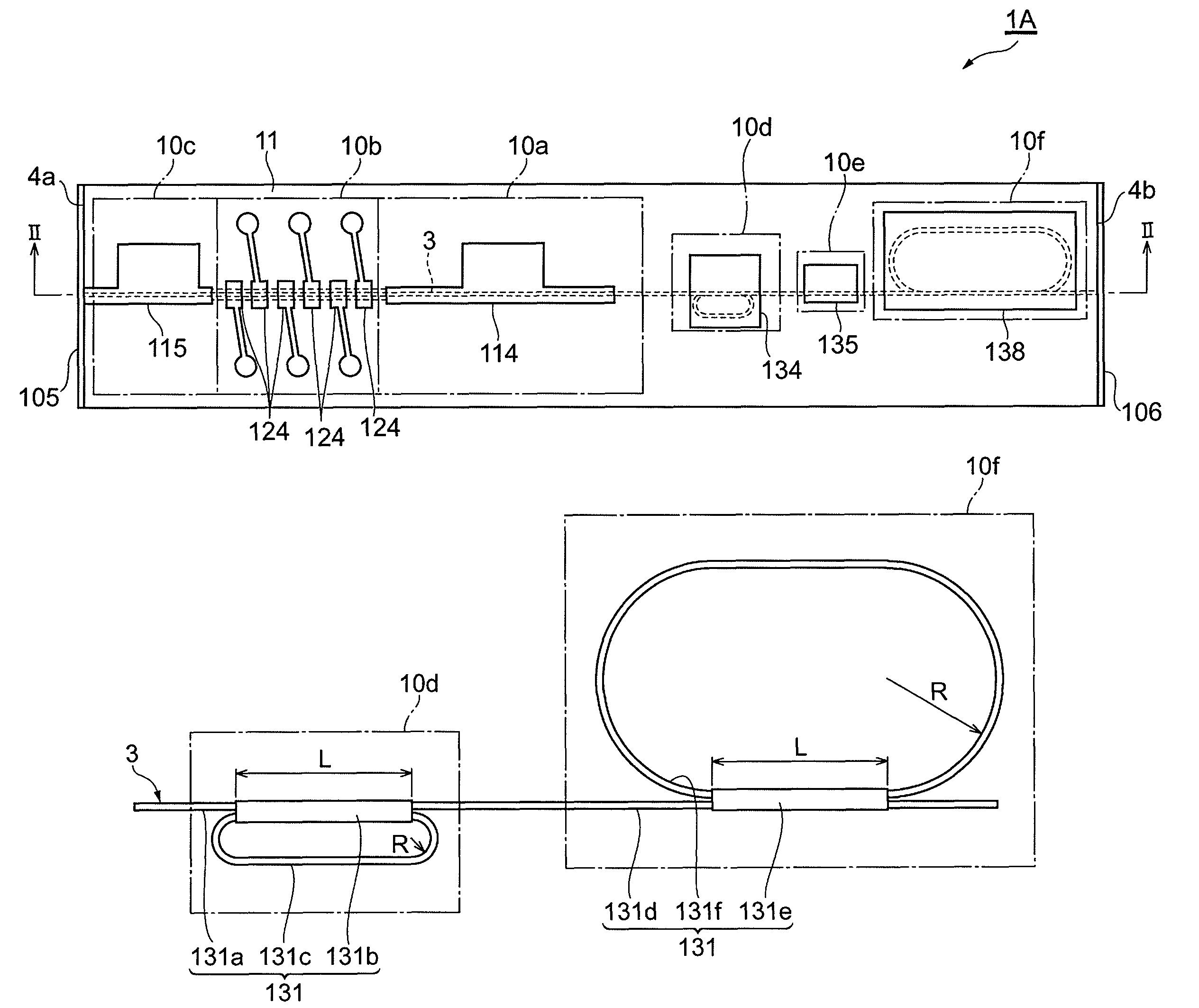
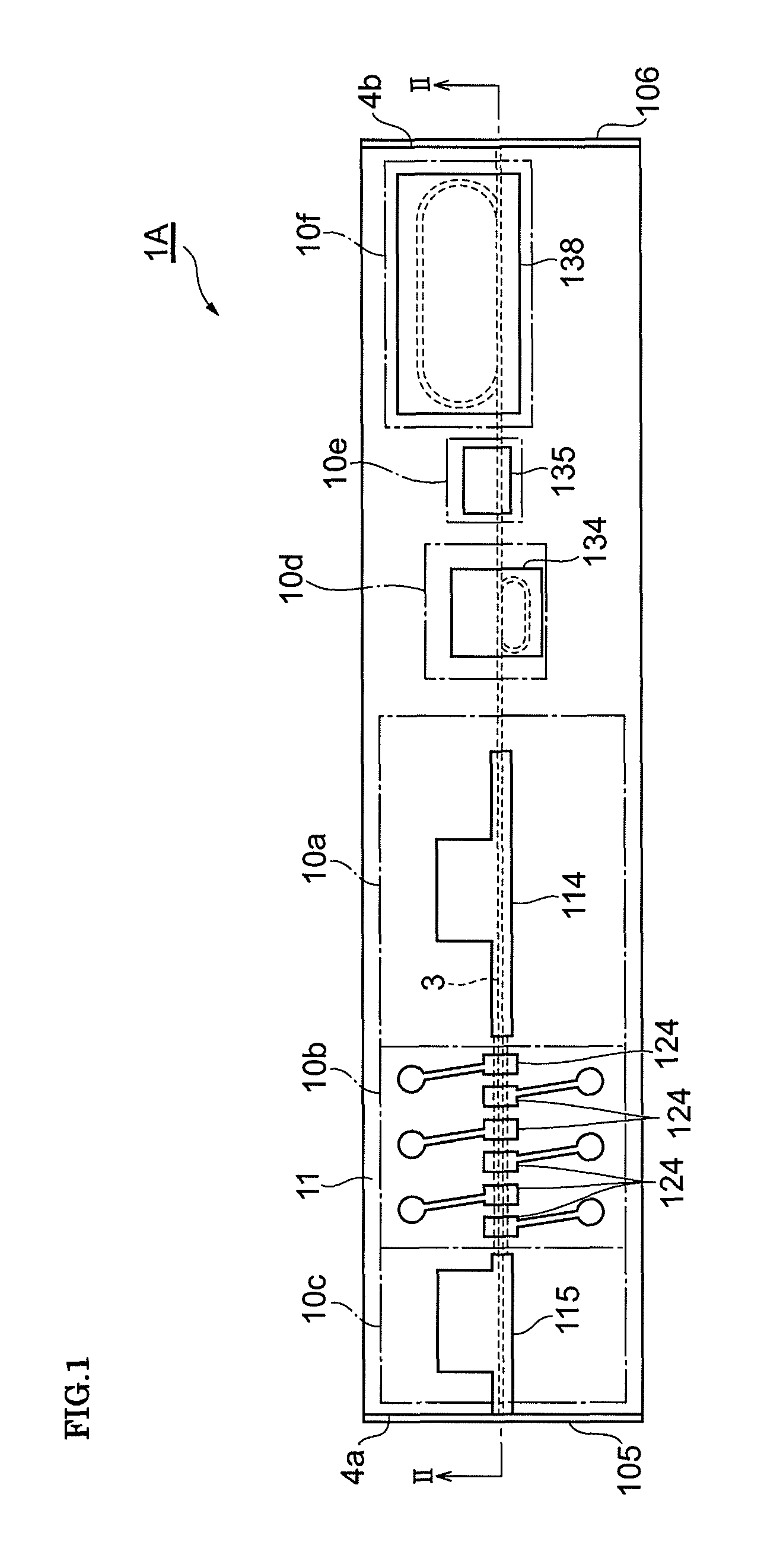
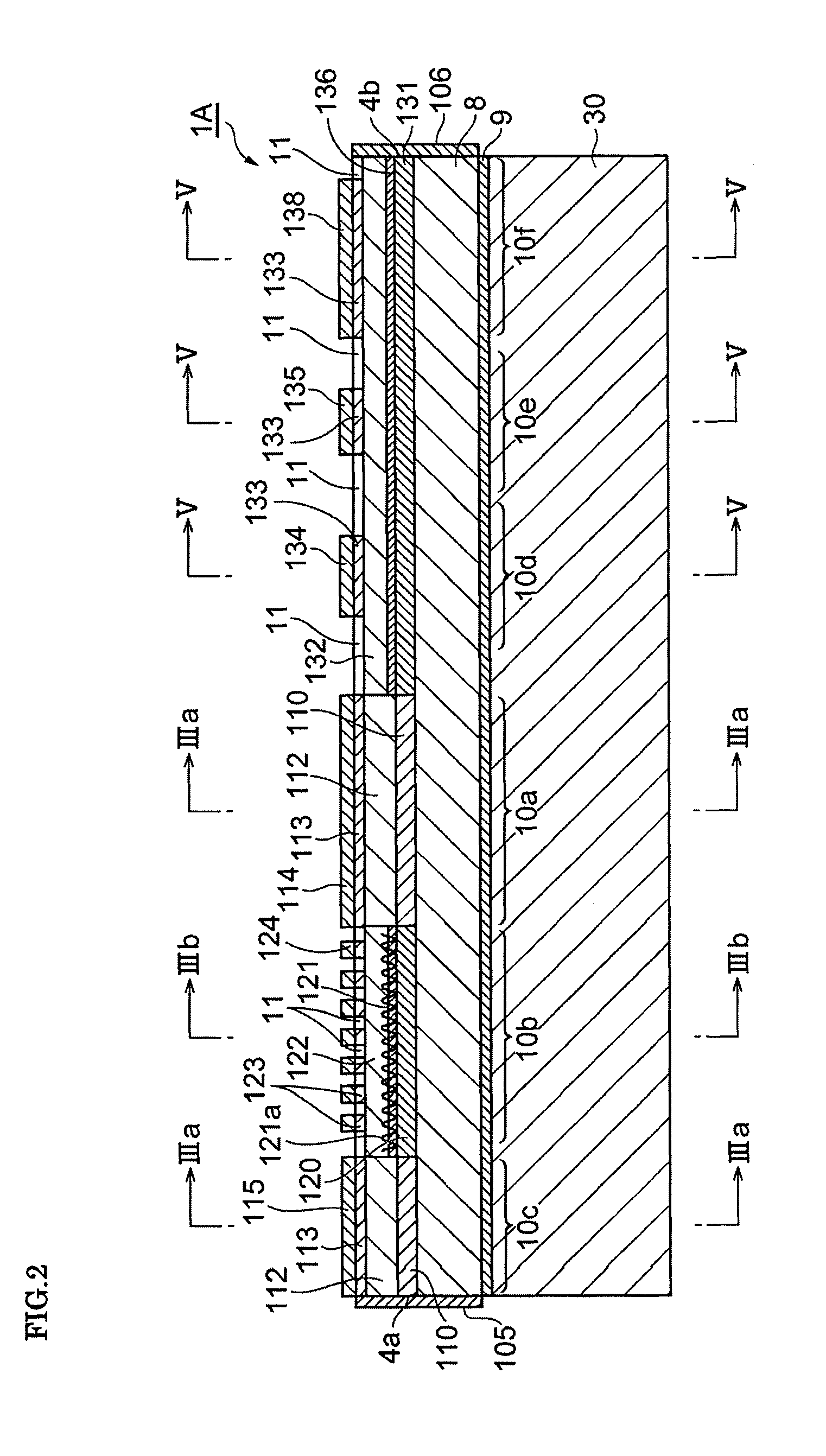
[0040]FIG. 1 is a plan view of a semiconductor laser 1A according to the embodiment of the present invention. FIG. 2 is a cross-sectional view taken along line II-II of the semiconductor laser 1A shown in FIG. 1. The semiconductor laser 1A is a wavelength tunable semiconductor laser.

[0041]Referring to FIGS. 1 and 2, the semiconductor laser 1A includes a gain region 10a, a distributed Bragg reflector (DBR) region 10b, an amplifier region 10c, a first ring resonator region 10d, a phase adjustment region (phase adjustment portion) 10e, and a second ring resonator region 10f. These regions 10a to 10f are formed on a common semiconductor substrate 8 as shown in FIG. 2, and arranged in a pr...


PUM


Abstract

A semiconductor laser includes a gain region; a distributed Bragg reflector (DBR) region including a diffraction grating; an end facet facing the DBR region with the gain region arranged therebetween; a first ring resonator including a first ring-like waveguide and a first optical coupler; a second ring resonator including a second ring-like waveguide and a second optical coupler; and an optical waveguide that is optically coupled to the end facet and extending in a predetermined optical-axis direction. The first and second ring resonators are optically coupled to the optical waveguide through the first and second optical couplers, respectively. Also, the DBR region, the gain region, and the end facet constitute a laser cavity. Further, the first ring resonator has a free spectral range different from a free spectral range of the second ring resonator.

Description

BACKGROUND OF THE INVENTION[0001]1. Field of the Invention[0002]The present invention relates to a semiconductor laser.[0003]2. Description of the Related Art[0004]Japanese Unexamined Patent Application Publication No. 2008-066318 discloses a wavelength tunable semiconductor laser. This wavelength tunable semiconductor laser includes a plurality of ring resonators having mutually different free spectral ranges (FSRs), and a gain region optically coupled to the plurality of ring resonators. More specifically, both ends of the gain region are respectively optically coupled to input ports of the individual ring resonators. Output ports of the ring resonators are optically coupled to a light emission end facet. The wavelength tunable semiconductor laser described in Japanese Unexamined Patent Application Publication No. 2008-066318 performs wavelength tuning by using vernier effect provided by the plurality of ring resonators having the mutually different FSRs.SUMMARY OF THE INVENTION[0...

Claims


Application Information

Patent Timeline
Patent Type & Authority Patents(United States)
IPC IPC(8): H01S5/00
CPCH01S5/06256H01S5/1071H01S5/142H01S5/50H01S5/1032H01S5/026H01S5/1212
Inventor FUKUDA, CHIE
Owner SUMITOMO ELECTRIC IND LTD
Why Eureka
Try Eureka