Organic el display panel and method of manufacturing the same

a technology of electroluminescence and display panels, which is applied in the direction of basic electric elements, electrical equipment, semiconductor devices, etc., can solve the problems of clogging of the nozzles of the inkjet head, hardly meeting the required standard, and the thickness of each layer formed by the ejection of ink hardly meets the required standard, etc., to achieve excellent image display performance, favorable production efficiency, and uniform thickness

Active Publication Date: 2014-07-15
JOLED INC
View PDF28 Cites 6 Cited by
  • Summary
  • Abstract
  • Description
  • Claims
  • Application Information

AI Technical Summary

Benefits of technology

[0017]Clogged nozzles, which cannot respond to changes made to the printing pattern on the substrate, could result in substrate losses and replacement of the inkjet head in the worst case. Even if there is a possibility of recovering the clogged nozzles, a user has to go to the trouble of detaching the inkjet head from the device, cleaning the inkjet head, and then attaching the inkjet head back to the device while maintaining alignment of the inkjet head with high accuracy (this attachment necessitates a recovery operation as well). This could significantly reduce production efficiency.
[0018]The present invention has been conceived in view of the above problems. The first aim of the present invention is to provide (i) an organic EL display panel that contains layers formed by an inkjet method with a uniform thickness, suppresses unevenness in light emission, and achieves excellent image display performance, and (ii) a method of manufacturing such an organic EL display panel.
[0019]The second aim of the present invention is to provide a method of manufacturing an organic EL display panel that can prevent clogging of nozzles in an inkjet head with favorable production efficiency.
[0021]According to the method of manufacturing the organic EL display panel pertaining to the present invention, concaves are formed in an upper surface of the bank in such a manner that along the column direction, each opening is sandwiched between a corresponding pair of adjacent concaves on the substrate. Furthermore, in steps (D) and (E), drops of first ink containing an organic material (material of the light-emitting layer) and a solvent are ejected into each concave. When the solvent in the drops of first ink that have been ejected into the concaves and openings has evaporated, the concentration of the vaporized solvent becomes uniform as compared with conventional cases, especially around both edges of each opening in the column direction. By drying the solvent in such an atmosphere with a uniform concentration of the vaporized solvent, the resultant light-emitting layers mostly have a uniform thickness. Hence, the organic EL display panel, as a whole, hardly brings about unevenness in light emission and therefore can achieve excellent image display performance.
[0022]Furthermore, in steps (D) and (E), the drops of first ink are ejected into (i) each column of openings through a predetermined number of nozzles among a plurality of nozzles disposed in an inkjet head, and (ii) each column of concaves through the rest of the plurality of nozzles other than the predetermined number of nozzles. Therefore, unlike conventional cases, the drops of first ink are ejected through every single nozzle. As described above, the concaves on the substrate are used by the nozzles for dummy ejection. That is, every single nozzle ejects the drops of first ink. This can alleviate the problem of clogging of the nozzles in the inkjet head, and allows manufacturing the organic EL display panel with favorable production efficiency.

Problems solved by technology

There are several problems in manufacturing organic EL display panels using a conventional inkjet method.
The first problem is that uniformity in the thickness of each layer formed by the ejected ink hardly meets the required standard.
The second problem is clogging of the nozzles in the inkjet head.

Method used


Image

  • Organic el display panel and method of manufacturing the same
  • Organic el display panel and method of manufacturing the same
  • Organic el display panel and method of manufacturing the same

Examples


embodiment 1

(Structure of Organic EL Display Panel 100)

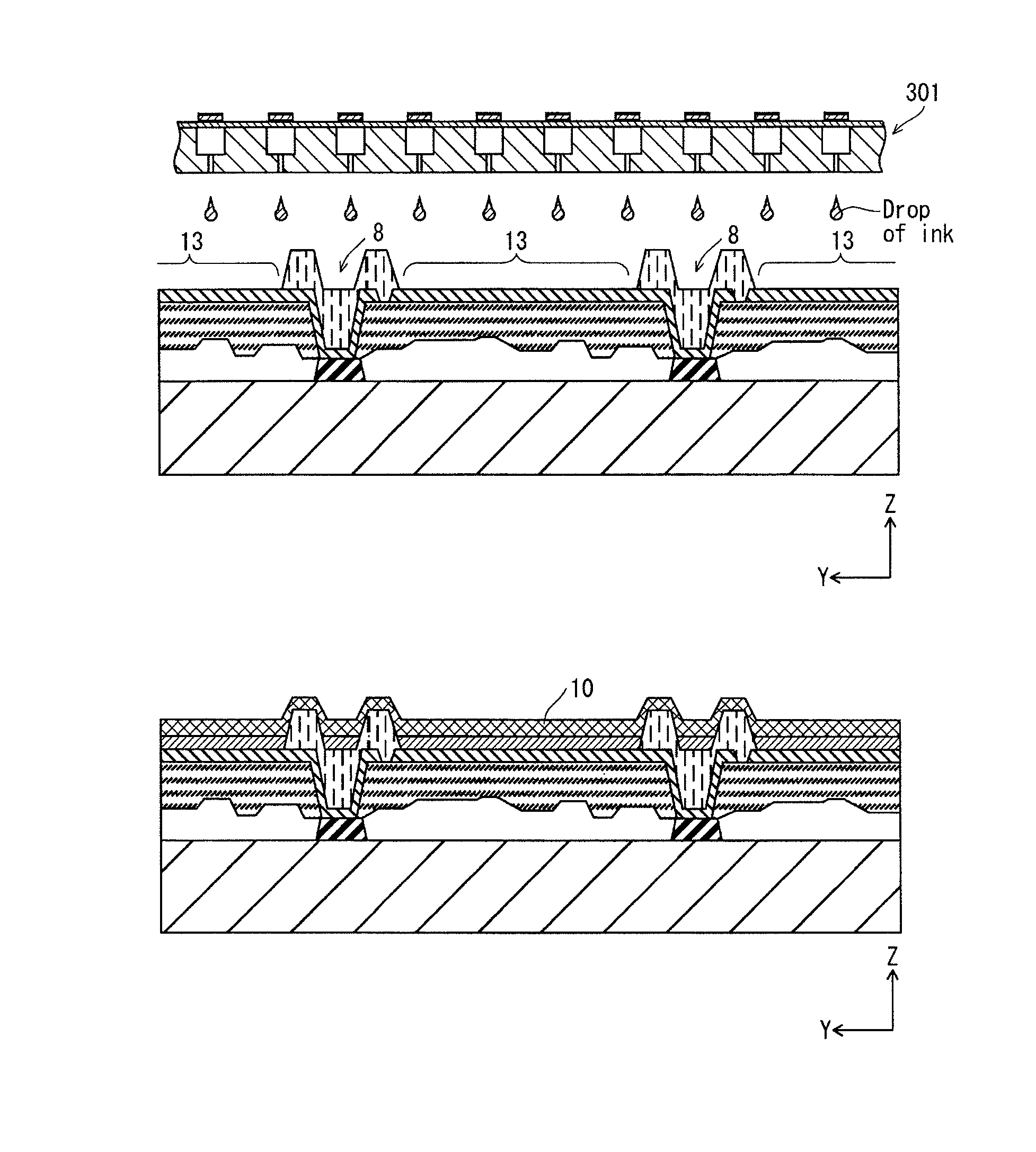
[0067]FIG. 1 is a cross-sectional view schematically showing the structure of an organic EL display panel 100 pertaining to Embodiment 1 of the present invention.

[0068]The organic EL display panel 100 shown in FIG. 1 includes, as subpixels (light-emitting pixels), organic EL elements 11a, 11b and 11c each having a light-emitting layer 9 corresponding to one of the following colors: R, G, and B. A combination of the three subpixels 11a, 11b and 11c constitutes one pixel. The organic EL elements 11a, 11b and 11c are adjacently arranged on an entirety of the organic EL display panel 100 in row (X) and column (Y) directions, i.e., in a matrix.

[0069]It goes without saying that the organic EL elements 11a, 11b and 11c may be configured to emit light of the same color.

[0070]On one main surface of a TFT substrate 1 (hereinafter, simply “substrate I”), a TFT wiring portion (TFT layer 2), a planarizing film 4, and a lower electrode 6 are layered in t...

embodiment 2

[0140]FIG. 12 is a schematic cross-sectional view showing the structure of an organic EL display panel 100A pertaining to Embodiment 2.

[0141]In the organic EL display panel 100A, a charge transport layer 9a is disposed beneath the light-emitting layer 9. The charge transport layer 9a improves luminous efficacy by suitably transporting a carrier toward the light-emitting layer 9. The charge transport layer 9a is formed in the wet process as with the light-emitting layer 9. More specifically, the charge transport layer 9a is formed by ejecting drops of ink containing a predetermined organic material (e.g., barium, phthalocyanine, lithium fluoride, or any combination of these materials) and solvent while maintaining the concentration of the vaporized solvent uniform along the column (Y) direction. This way, the charge transport layer 9a has a favorably uniform thickness. After the charge transport layer 9a is formed, the light-emitting layer 9 is formed thereon in the same manner as Em...

embodiment 3

[0144]FIG. 14 is a schematic cross-sectional view showing the structure of an organic EL display panel 100B pertaining to Embodiment 3.

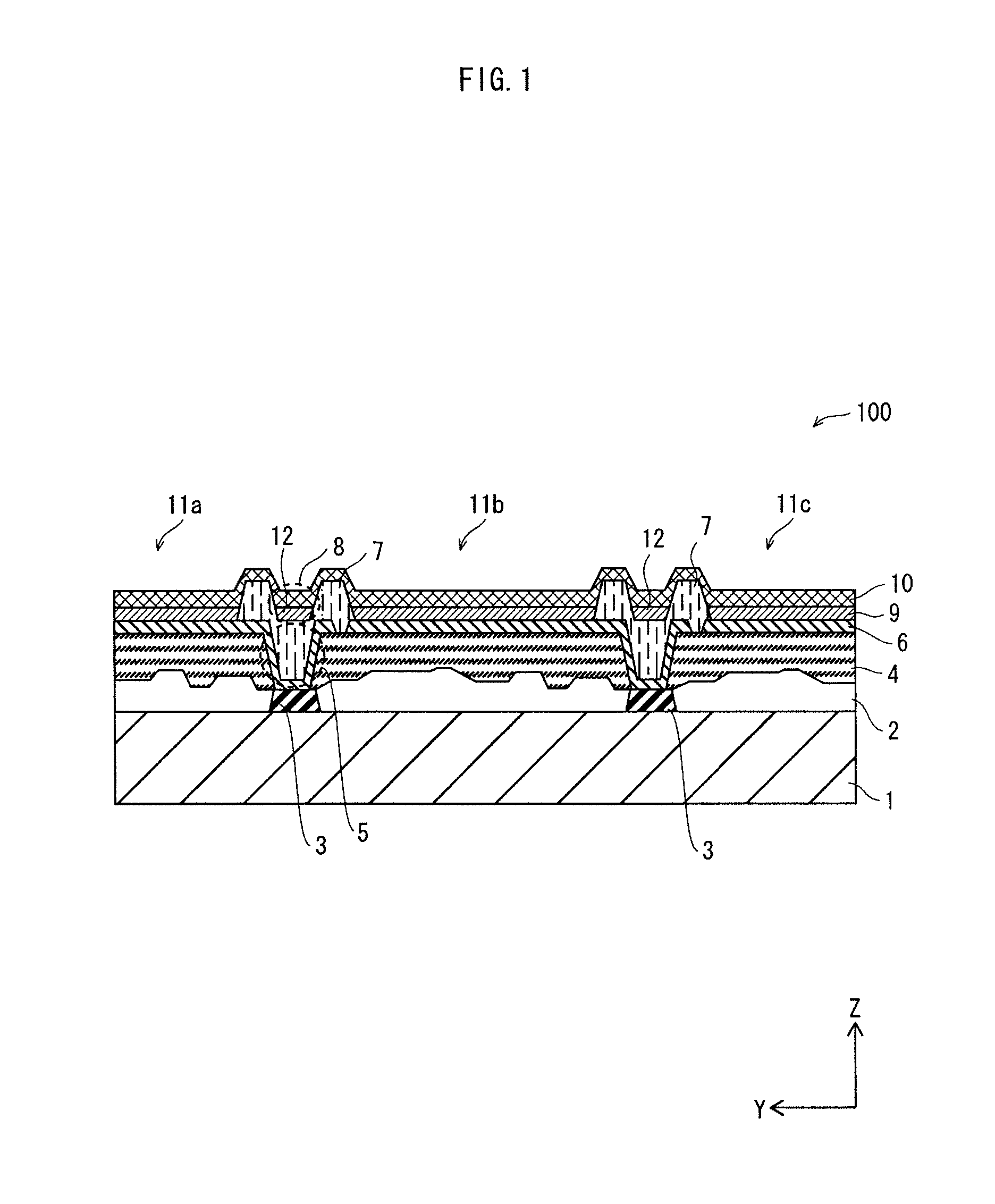
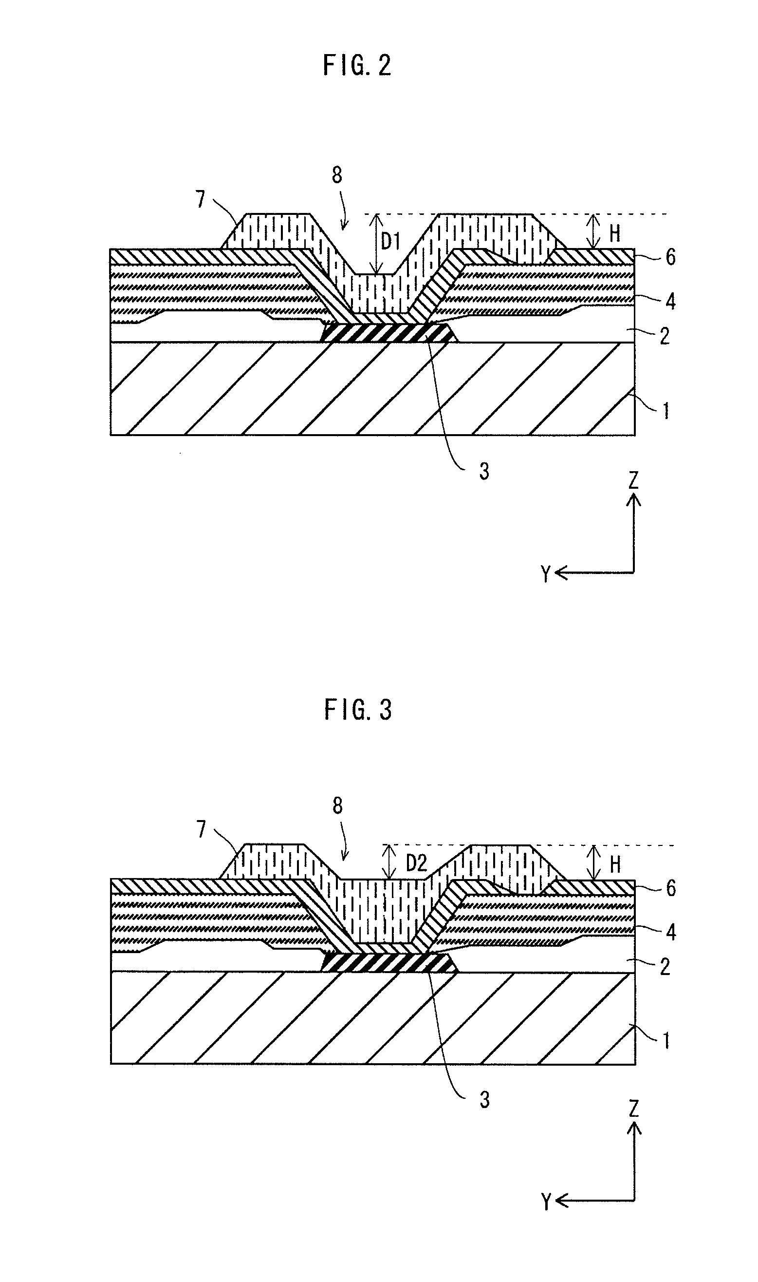
[0145]In the organic EL display panel 100B, the contact holes 5 are not formed. Accordingly, the concaves 8 of the bank 7 are formed only through adjustment of the shape of the bank 7. Here, as shown in FIG. 15, the depth D3 of each concave 8 is adjusted to be the same as the height H of the bank 7. Alternatively, the depth D3 may be adjusted to be smaller than or larger than the height H.

[0146]In this structure also, the same drops of ink are ejected into the openings 13 and the concaves 8 in the wet process of the inkjet method during the step of forming the light-emitting layer 9. As a result, the concentration of the vaporized solvent is made uniform while the ink is being dried, and the light-emitting layer 9 having a uniform thickness is formed.

[0147]Furthermore, the nozzles 3030 in the inkjet head 30 are caused to eject the ink into the concav...


PUM


Abstract

An organic electroluminescence display panel includes a thin-film transistor layer above a substrate. A planarizing film is above the thin-film transistor layer with contact holes being formed in the planarizing film. A bank is above the planarizing film. The bank includes openings arranged in rows and columns that define regions for forming organic electroluminescence elements. Each opening is between a pair of adjacent concaves in one of the columns. The concaves are formed in an upper surface of the bank and sunken into the contact holes. The upper surface of the bank has repellency. A light-emitting layer is formed in each opening by ejecting drops of an ink from nozzles of an inkjet head into the openings while moving the inkjet head relative to the substrate. The nozzles further eject drops of the ink into the concaves when above the concaves for ejecting the drops of the ink through every nozzle.

Description

CROSS REFERENCE TO RELATED APPLICATION[0001]This is a continuation application of PCT Application No. PCT / JP2010 / 004311 filed on Jun. 30, 2010, designating the United States of America, the disclosure of which, including the specification, drawings and claims, is incorporated herein by reference in its entirety.BACKGROUND OF THE INVENTION[0002]1. Field of the Invention[0003]The present invention relates to an organic electroluminescence (EL) display panel including organic EL elements, which are electric light-emitting elements, and in particular to a technical improvement in an ejection process using an inkjet head.[0004]2. Description of the Related Art[0005]Organic EL elements, which have come into practical use in recent years, are current-driven light-emitting elements. Each organic EL element has the following basic structure. A light-emitting layer that includes an organic light-emitting material is disposed between a pair of electrodes, i.e., an anode and a cathode. When dri...

Claims


Application Information

Patent Timeline
Patent Type & Authority Patents(United States)
IPC IPC(8): H01L21/00
CPCH01L51/56H01L51/0005H01L27/3246H10K59/122H10K71/135H10K71/00H10K50/30
Inventor TAKEUCHI, TAKAYUKI
Owner JOLED INC
Why Eureka
Try Eureka