Semiconductor structure with dispersedly arranged active region trenches

a technology of active region trenches and semiconductors, which is applied in the direction of semiconductor devices, semiconductor/solid-state device details, electrical apparatus, etc., can solve the problem of insufficient rated output current value, and achieve the effect of increasing the exposed surface area

Active Publication Date: 2014-07-15
TAIWAN SEMICONDUCTOR COMPANY LIMITED
View PDF2 Cites 0 Cited by
  • Summary
  • Abstract
  • Description
  • Claims
  • Application Information

AI Technical Summary

Benefits of technology

[0019]Accordingly, a major object of the present invention is to provide a semiconductor structure with dispersedly arranged active region trenches, which has a plurality of active region trenches formed in the epitaxial layer and these active region trenches are arranged in a dispersed manner. Such structure is capable to increase the exposed surface area of the epitaxial layer such that a desired current output might be generated by using a smaller forward bias voltage.

Problems solved by technology

Because the conventional semiconductor structure has the disadvantage of low current output under forward bias and usually needs a higher forward bias voltage to achieve the desired current output, thus, there exists the problem of insufficient rated output current value in the prior art.

Method used


Image

  • Semiconductor structure with dispersedly arranged active region trenches
  • Semiconductor structure with dispersedly arranged active region trenches
  • Semiconductor structure with dispersedly arranged active region trenches

Examples


Embodiment Construction

[0025]There are various embodiments of the composite regeneration membrane in accordance with the present invention, which are not repeated hereby. The preferred embodiment is mentioned in the following paragraph as an example. It should be understood by those skilled in the art that the preferred embodiments disclosed in the following paragraph are merely an example instead of restricting the scope of the invention itself.

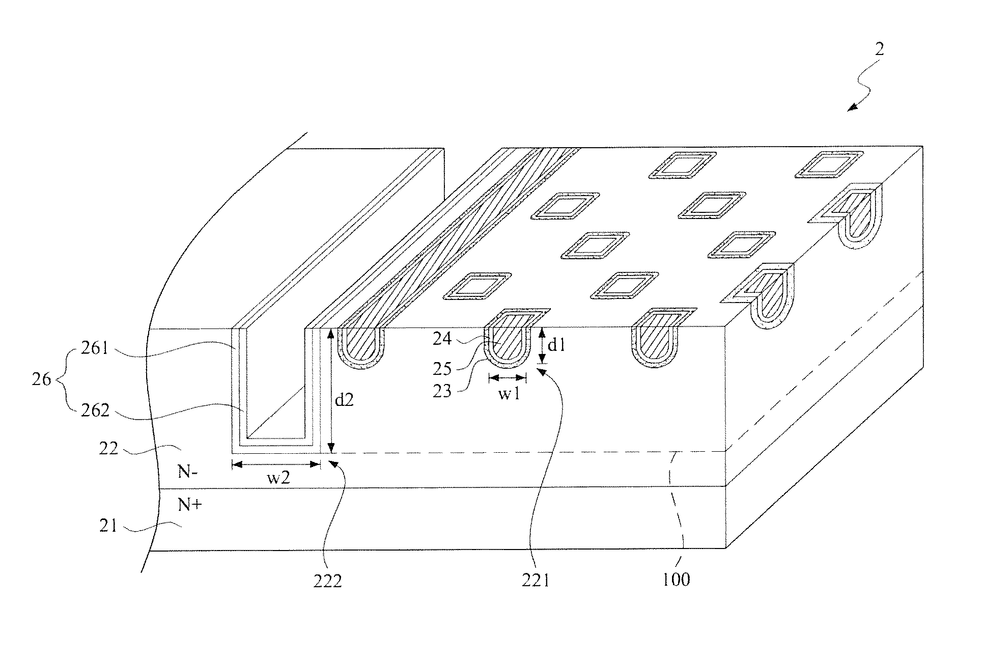
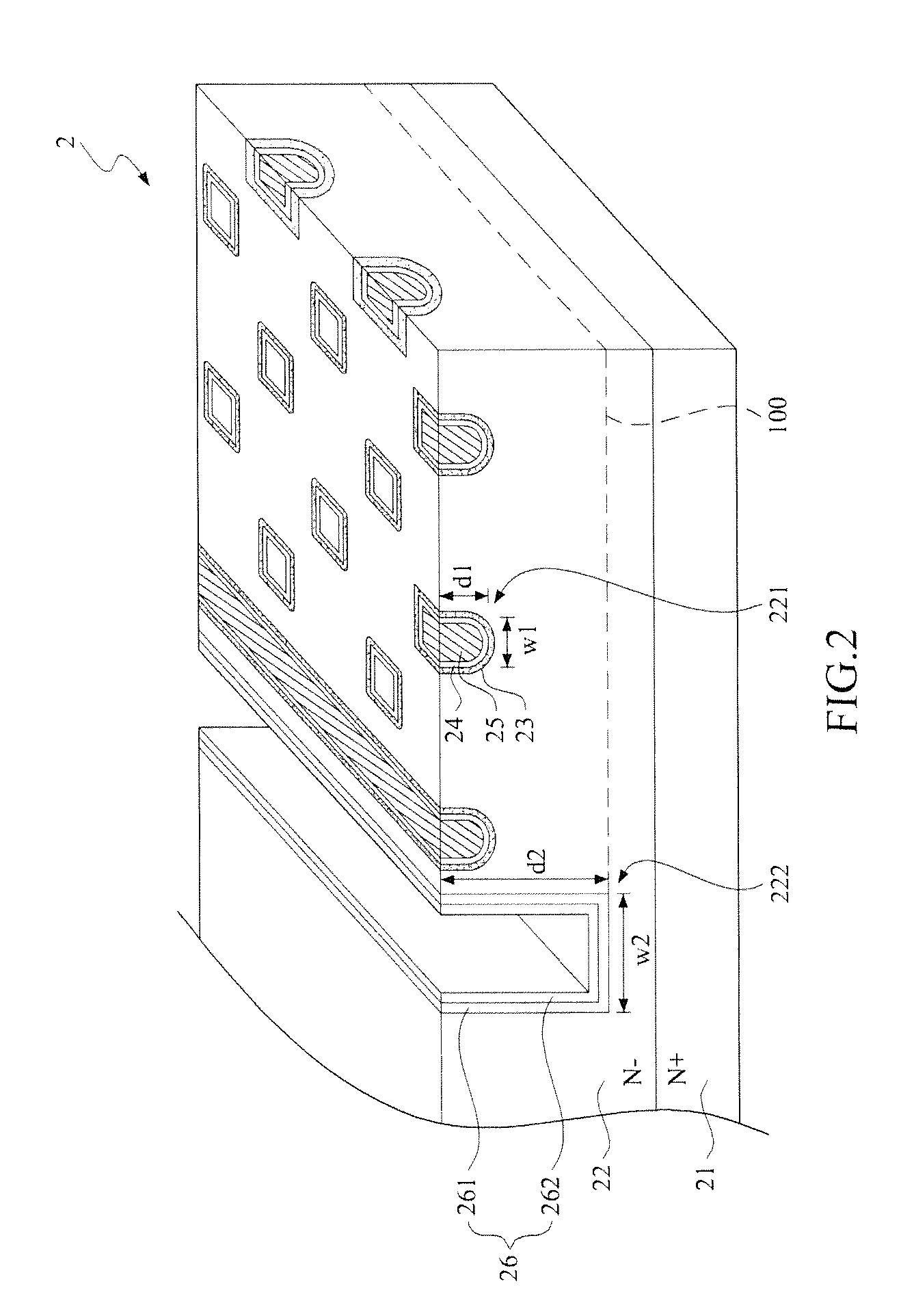
[0026]Please refer to both FIG. 2 and FIG. 3, wherein FIG. 2 is a schematic view of a semiconductor structure with dispersedly arranged active region trenches in accordance with a first embodiment of the present invention, and FIG. 3 is a schematic view showing the arrangement of the active region trenches of the first embodiment of the present invention. As show in FIG. 2 and FIG. 3, the semiconductor structure 2 comprises a semiconductor substrate 21, an epitaxial layer 22, an ion implantation layer 23, an active region dielectric layer 24, a polysilicon layer 2...


PUM


Abstract

A semiconductor structure with dispersedly arranged active region trenches is provided. The semiconductor structure comprises a semiconductor substrate, an epitaxial layer, and an active region dielectric layer. The semiconductor substrate is doped with impurities of a first conductive type having a first impurity concentration. The epitaxial layer is doped with impurities of the first conductive type having a second impurity concentration and is formed on the semiconductor substrate. The epitaxial layer has a plurality of active region trenches formed therein being arranged in a dispersed manner. The active region dielectric layer covers a bottom and a sidewall of the active region trenches. Wherein, the active region trench has an opening in a tetragonal shape on a surface of the epitaxial layer, and the first impurity concentration is greater than the second impurity concentration.

Description

FIELD OF THE INVENTION[0001]The present invention relates to a semiconductor structure with dispersedly arranged active region trenches, and more particularly relates to a semiconductor structure with active region trenches arranged in the epitaxial layer in a dispersed manner.BACKGROUND OF THE INVENTION[0002]For a long time, schottky diode has been an important power device featuring a metal-semiconductor junction to create a schottky barrier so as to provide the function of rectification. With the characteristics of high switching speed and rectification, the schottky diode has been widely applied to high speed switching power devices, digital computers, and output regulators[0003]However, the present schottky diodes fabricated by using semiconductor structures has the disadvantages of low reverse breakdown voltage and large reverse leakage current. In addition, the reverse current increases with increasing temperature to result in the problem of thermal instability. Thus, schottk...

Claims


Application Information

Patent Timeline
Patent Type & Authority Patents(United States)
IPC IPC(8): H01L29/06
CPCH01L29/0692H01L21/26586H01L29/47H01L29/8725H01L29/872
Inventor HUANG, CHAO-HSINCHUANG, CHIH-CHIANG
Owner TAIWAN SEMICONDUCTOR COMPANY LIMITED
Why Eureka
Try Eureka