Method of forming conformal metal silicide films

a technology of conformal metal silicide and film, which is applied in the direction of coatings, chemical vapor deposition coatings, capacitors, etc., can solve the problems of increasing the serial resistance of inner electrodes (plugs, trench-drams, etc., and the difficulty of very deep trenches

Inactive Publication Date: 2014-07-22
TOKYO ELECTRON LTD
View PDF13 Cites 1 Cited by
  • Summary
  • Abstract
  • Description
  • Claims
  • Application Information

AI Technical Summary

Problems solved by technology

Both applications suffer from the fact that the serial resistance of the inner electrode (plug, deep trench-DRAM) or vias (stacked DRAM) increases with the square of the inverse ground rule.
Conformal deposition of these films is usually required and this is very challenging for very deep trenches.

Method used


Image

  • Method of forming conformal metal silicide films
  • Method of forming conformal metal silicide films
  • Method of forming conformal metal silicide films

Examples


Embodiment Construction

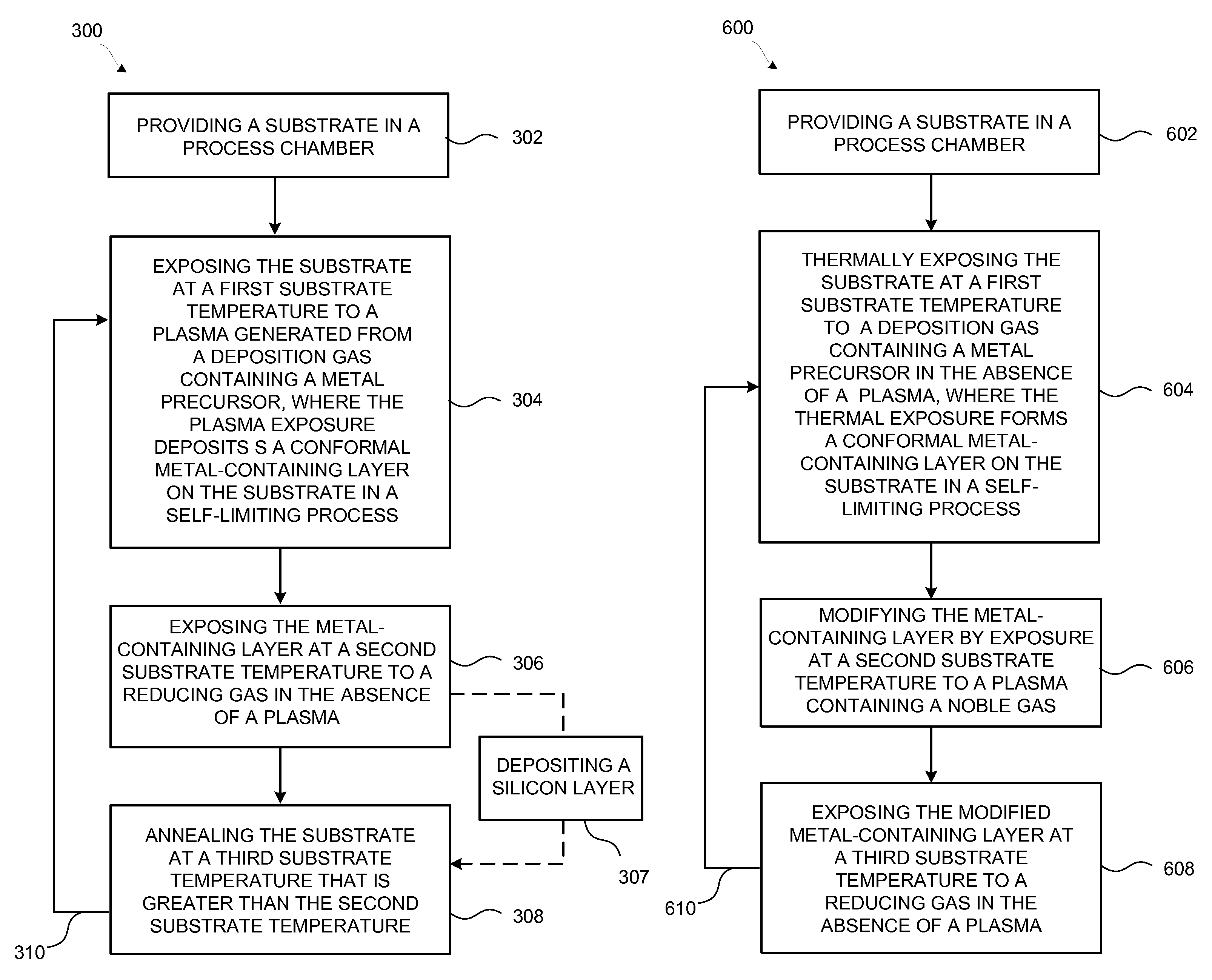
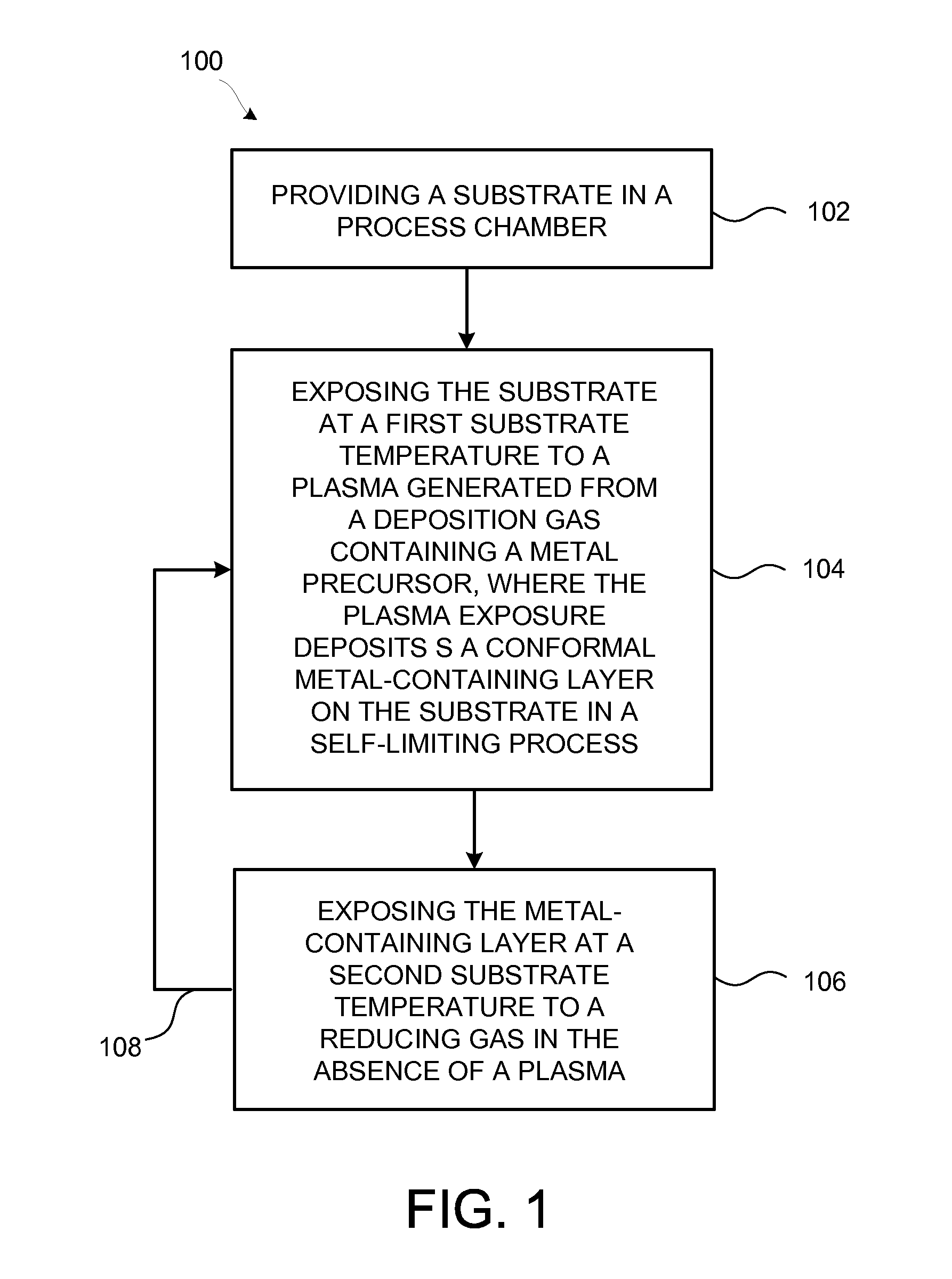
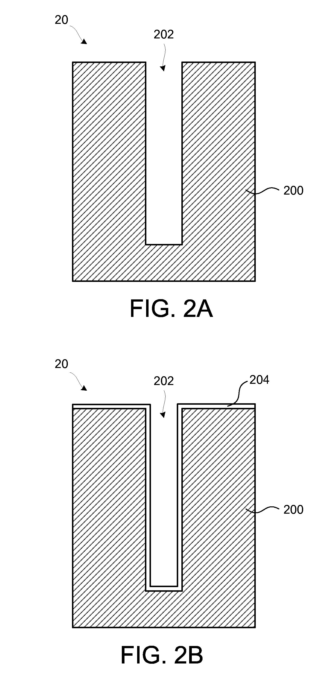
[0017]Methods for forming conformal metal silicide layers on substrates are disclosed in several embodiments. The metal silicide layers can, for example, include a titanium silicide (e.g., TiSix), a molybdenum silicide (e.g., MoSix), a tungsten silicide (WSix), a tantalum silicide (e.g., TaSix), or a vanadium silicide (VSix), or a combination of two or more thereof.

[0018]One skilled in the relevant art will recognize that the various embodiments may be practiced without one or more of the specific details, or with other replacement and / or additional methods, materials, or components. In other instances, well-known structures, materials, or operations are not shown or described in detail to avoid obscuring aspects of various embodiments of the invention. Similarly, for purposes of explanation, specific numbers, materials, and configurations are set forth in order to provide a thorough understanding of the invention. Furthermore, it is understood that the various embodiments shown in ...


PUM

PropertyMeasurementUnit
depthaaaaaaaaaa
depthaaaaaaaaaa
depthaaaaaaaaaa

Abstract

A method is provided for forming a metal silicide layer on a substrate. According to one embodiment the method includes providing the substrate in a process chamber, exposing the substrate at a first substrate temperature to a plasma generated from a deposition gas containing a metal precursor, where the plasma exposure forms a conformal metal-containing layer on the substrate in a self-limiting process. The method further includes exposing the metal-containing layer at a second substrate temperature to a reducing gas in the absence of a plasma, where the exposing steps are alternatively performed at least once to form the metal silicide layer, and the deposition gas does not contain the reducing gas. The method provides conformal metal silicide formation in deep trenches with high aspect ratios.

Description

CROSS-REFERENCE TO RELATED APPLICATIONS[0001]This application is related to and claims priority to U.S. Provisional application Ser. No. 61 / 591,843 (Ref no. TTCA-389Pro) filed on Jan. 27, 2012, the entire contents of which are herein incorporated by reference.FIELD OF THE INVENTION[0002]The present invention generally relates to forming conformal metal silicide films on a substrate using vapor deposition. The substrate may include deep trenches with high aspect ratios used in semiconductor devices.BACKGROUND OF THE INVENTION[0003]In the semiconductor industry, the minimum feature sizes of microelectronic devices are approaching the deep sub-micron regime to meet the demand for faster, lower power microprocessors and digital circuits. Low resistivity refractory metal silicide layers, for instance, are widely used as part of the gate stack in dynamic random access memory (DRAM) and enhanced DRAM (EDRAM) manufacturing. Another application for low resistivity metal silicide layers is in...

Claims


Application Information

Patent Timeline
Patent Type & Authority Patents(United States)
IPC IPC(8): H01L21/44
CPCH01L21/76898C23C16/42C23C16/45538H01L21/28518H01L21/28562H01L28/91H01L29/66181H01L21/76858
Inventor HASEGAWA, TOSHIOTADA, KUNIHIROYAMASAKI, HIDEAKIO'MEARA, DAVID L.LEUSINK, GERRIT J.
Owner TOKYO ELECTRON LTD
Why Eureka
Try Eureka