Double-gate FET with planarized surfaces and self-aligned silicides

a technology of planarized surfaces and silicides, applied in the direction of semiconductor devices, electrical devices, transistors, etc., can solve the problems of difficult to form thin vertical pillars (e.g., 10 nm) that are free of reactive ion etching damage, and difficult to keep the top and bottom gate oxides at the same thickness

Inactive Publication Date: 2003-11-04
GLOBALFOUNDRIES INC
View PDF14 Cites 86 Cited by
  • Summary
  • Abstract
  • Description
  • Claims
  • Application Information

AI Technical Summary

Problems solved by technology

However there is no conventional method of making a double-gate MOSFET structure which has both the top and bottom gate self-aligned to the source / drain suicides and which produces a planarized surface after the formation of the source / drain and gate structures.
However, with this method, it is difficult to form thin vertical pillars (e.g., 10 nm) that are free of reactive ion etching (RIE) damage and to maintain good thickness control.
However, with this method, it is difficult to keep the top and bottom gate oxides at the same thickness and to align the gates with each other.
However, this method also suffers silicon thickness control problems and gate alignment problems.

Method used


Image

  • Double-gate FET with planarized surfaces and self-aligned silicides
  • Double-gate FET with planarized surfaces and self-aligned silicides
  • Double-gate FET with planarized surfaces and self-aligned silicides

Examples


Embodiment Construction

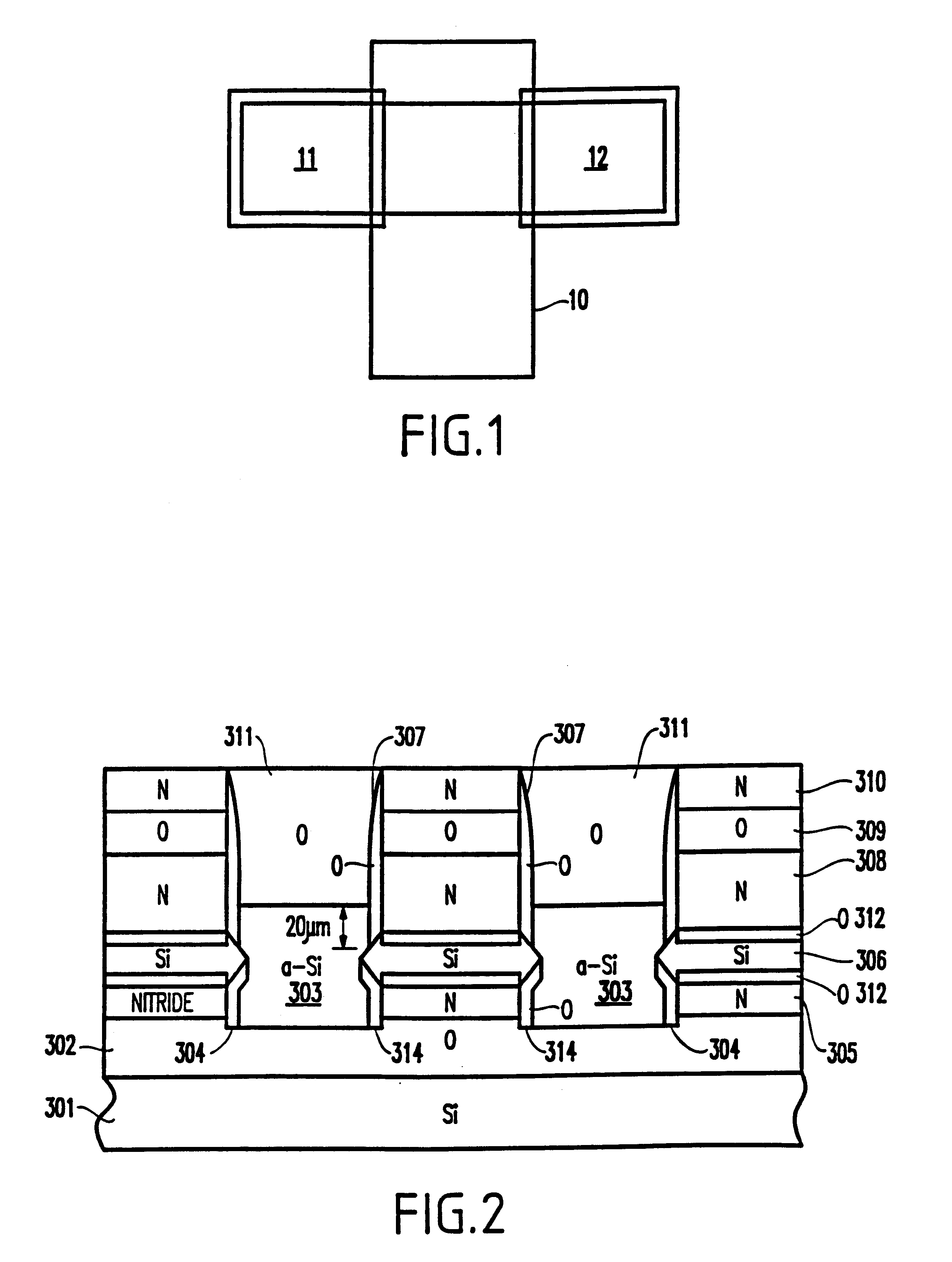
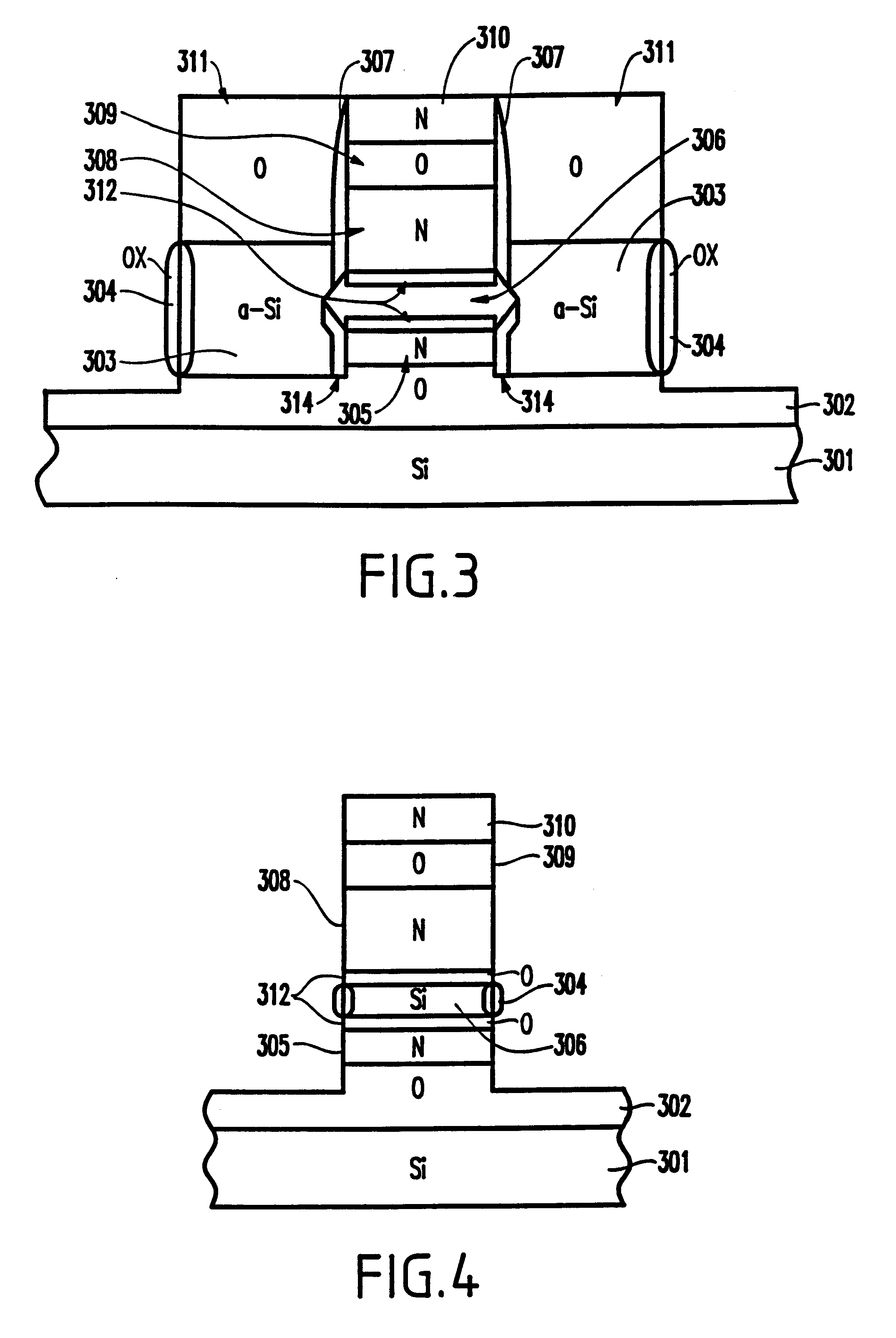
As discussed above, the invention provides a structure and method for fabricating a double-gate field effect transistor (FET) with a planarized surface and with gate regions which are self-aligned to the source drain. The silicide regions over the gate, source and drain are formed in a single self-aligned (salicide) processing step. The planarized surface of the inventive structure is important for subsequent processing which needs a level surface.

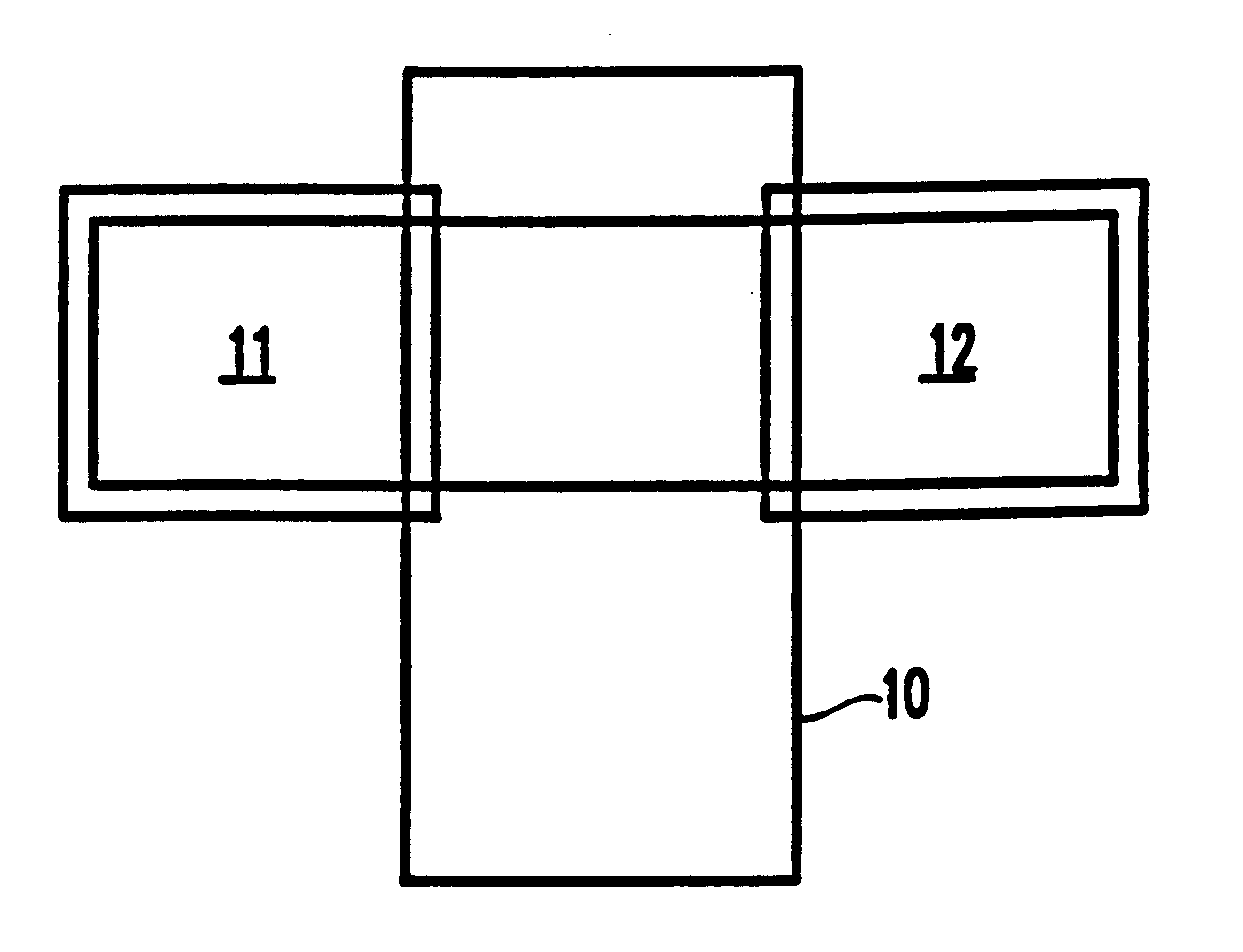
FIG. 1 illustrates a top view of the inventive structure which includes a gate 10 and source and drain and regions 11, 12. FIGS. 2-11 illustrate the various stages of production of the inventive structure and the process for forming the inventive structure. While a single process for the invention is disclosed below, as would be known by one ordinarily skilled in the art given this disclosure, many similar processes may be substituted at various points of the inventive method without departing from the concept of the invention to achieve a...


PUM


Abstract

It is, therefore, an object of the present invention to provide a structure and method for an integrated circuit comprising a first gate, a second gate, and source and drain regions adjacent the first and second gates, wherein the structure has a planar upper structure and the first gate, source and drain regions are silicided in a single self-aligned process (salicide).

Description

1. Field of the InventionThe present invention generally relates to metal oxide semiconductor field effect transistors (MOSFETS) and more particularly to a double-gate MOSFET that has several advantages over conventional single-gate MOSFETs.2. Description of the Related ArtIt is conventionally known that a double-gate MOSFET has several advantages of over conventional single-gate MOSFET structures (dual-gates are side by side, while double-gates form a top and bottom gate structure). For example, the double-gate MOSFET structure has higher transconductance, lower parasitic capacitance and superior short-channel characteristics when compared to single-gate MOSFET structures. Various simulations have shown that a 30 nm channel double-gate MOSFET will show very high transconductance (2300 mS / mm) and very fast switching speeds. Moreover, good short-channel characteristics are obtained down to a 20 nm channel length, which does not require doping. Therefore, double-gate MOSFETs circumven...

Claims


Application Information

Patent Timeline
Patent Type & Authority Patents(United States)
IPC IPC(8): H01L29/786H01L21/02H01L21/336H01L27/12H01L29/66
CPCH01L27/1203H01L29/66772H01L29/78696H01L29/78648H01L29/78618
Inventor COHEN, GUY M.WONG, HON-SUM P.
Owner GLOBALFOUNDRIES INC
Why Eureka
Try Eureka