Three-dimensional semiconductor memory devices using direct strapping line connections

a three-dimensional semiconductor and memory device technology, applied in the field of three-dimensional semiconductor memory devices, can solve the problems of general limited degree of integration and the cost of process equipment needed to increase the fineness of patterns, and achieve the effect of reducing the cost of process equipmen

Active Publication Date: 2014-08-12
SAMSUNG ELECTRONICS CO LTD
View PDF18 Cites 26 Cited by
  • Summary
  • Abstract
  • Description
  • Claims
  • Application Information

AI Technical Summary

Problems solved by technology

In typical two-dimensional or planar semiconductor memory devices, the degree of integration is generally limited by the area occupied by a unit memory cell, which may be limited by fine pattern forming technology.
In particular, the expense of process equipment needed to increase pattern fineness may act as a practical limitation on increasing integration for two-dimensional or planar semiconductor memory devices.

Method used


Image

  • Three-dimensional semiconductor memory devices using direct strapping line connections
  • Three-dimensional semiconductor memory devices using direct strapping line connections
  • Three-dimensional semiconductor memory devices using direct strapping line connections

Examples


Embodiment Construction

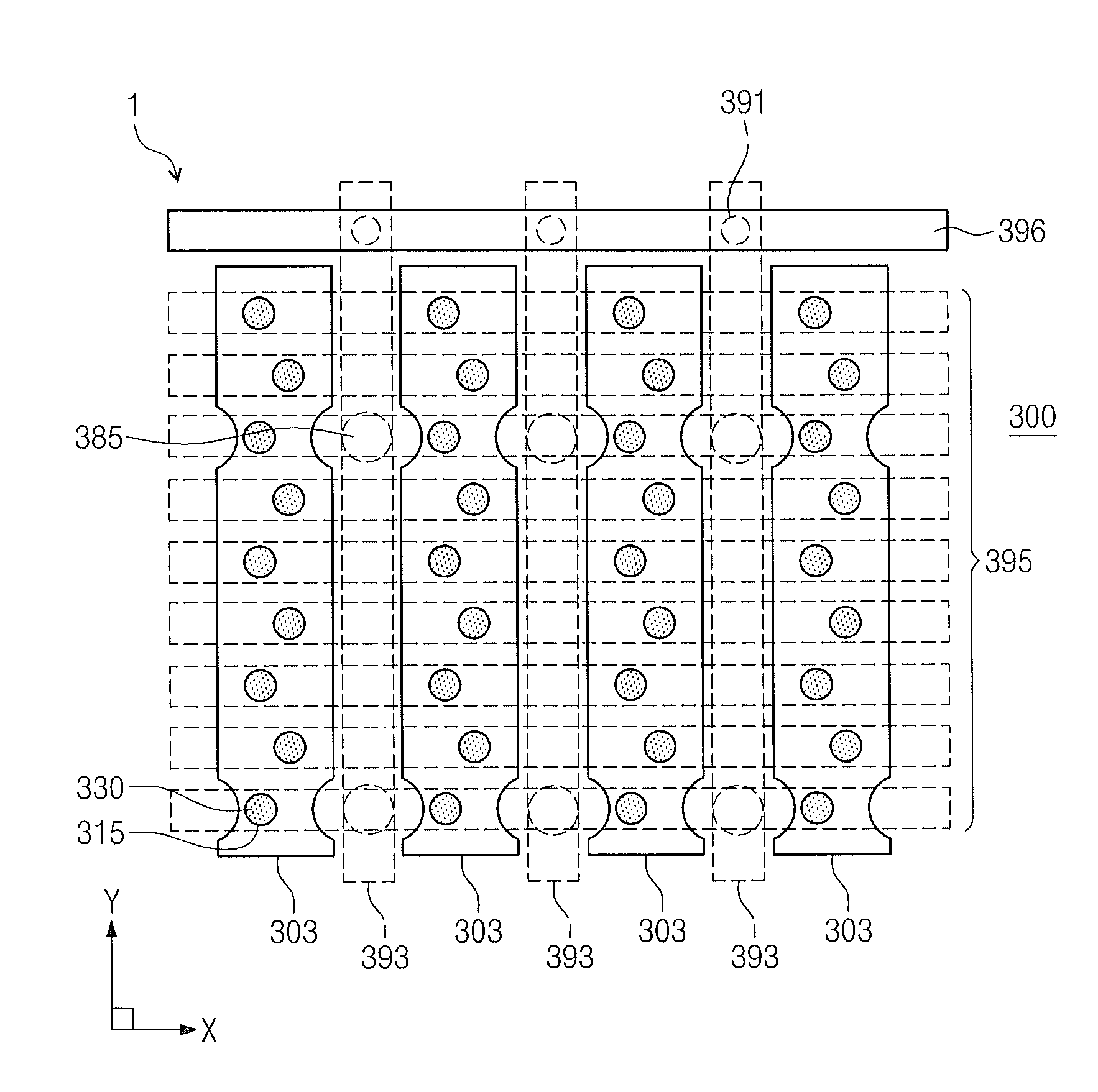
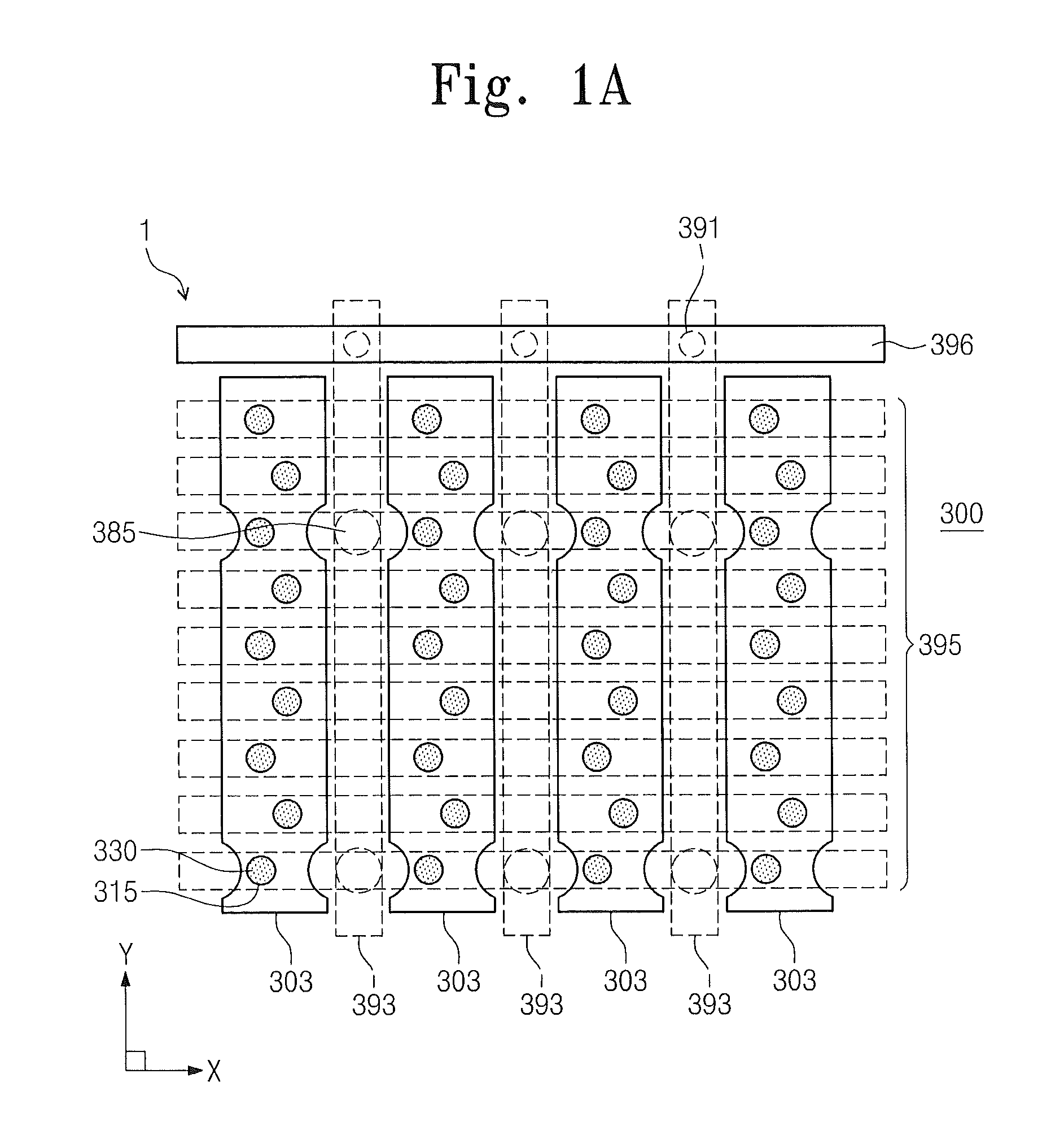
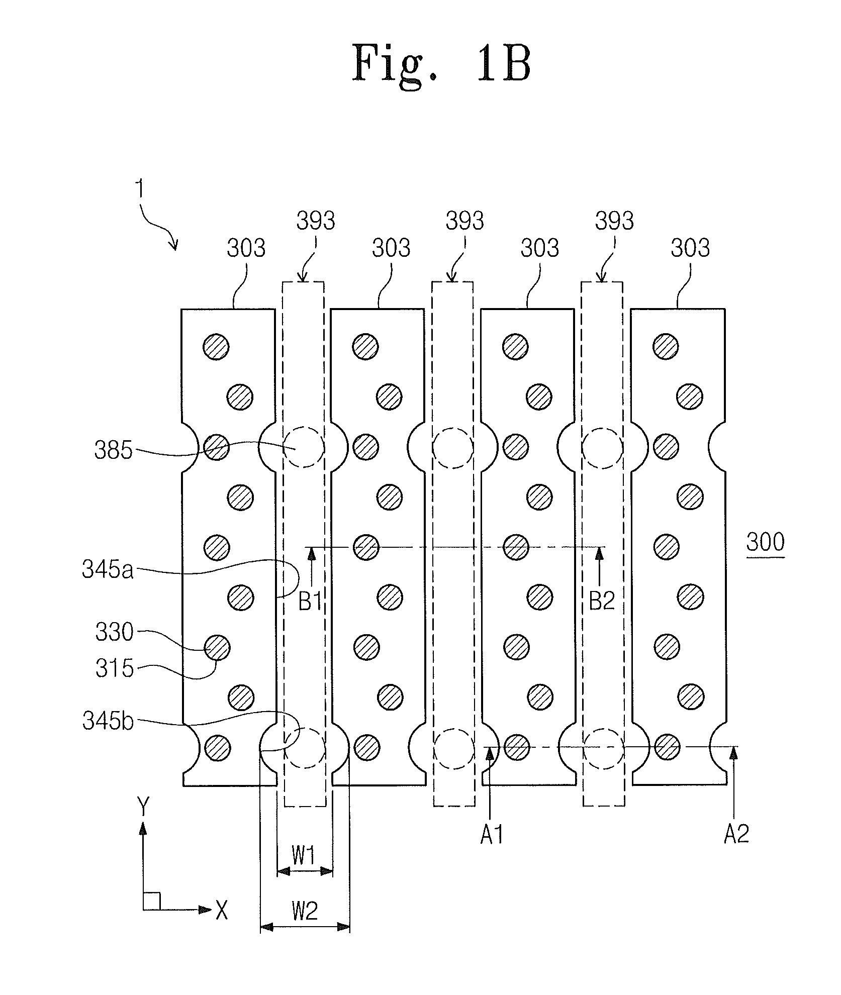
[0023]Example embodiments of the subject matter will now be described more fully with reference to the accompanying drawings, in which example embodiments are shown. Example embodiments of the subject matter may, however, be embodied in many different forms and should not be construed as being limited to the embodiments set forth herein; rather, these embodiments are provided so that this disclosure will be thorough and complete, and will fully convey the concept of example embodiments to those of ordinary skill in the art. In the drawings, the thicknesses of layers and regions are exaggerated for clarity. Like reference numerals in the drawings denote like elements, and thus their description will be omitted.

[0024]It will be understood that when an element is referred to as being “connected” or “coupled” to another element, it can be directly connected or coupled to the other element or intervening elements may be present. In contrast, when an element is referred to as being “direc...


PUM


Abstract

Memory devices include a plurality of elongate gate stacks extending in parallel on a substrate and at least one insulation region disposed in a trench between adjacent ones of the gate stacks. The at least one insulation region has linear first portions having a first width and widened second portions having a second width greater than the first width. A common source region is disposed in the substrate underlying the at least one insulation region. The devices further include respective conductive plugs passing through respective ones of the widened second portions of the at least one insulation region and electrically connected to the common source region and at least one strapping line disposed on the conductive plugs between the adjacent ones of the gate stacks and in direct contact with the conductive plugs.

Description

CROSS-REFERENCE TO RELATED APPLICATIONS[0001]This U.S. non-provisional patent application claims priority under 35 U.S.C. §119 to Korean Patent Application No. 10-2011-0067478, filed on Jul. 7, 2011, in the Korean Intellectual Property Office, the entire contents of which are hereby incorporated by reference.BACKGROUND OF THE INVENTION[0002]Embodiments of the subject matter relate generally to semiconductor devices and, more particularly, to three-dimensional semiconductor memory devices and methods of fabricating the same.[0003]Due to their small size, multifunctional capabilities and / or low cost, semiconductor devices are important elements in the electronic industry. Higher integration of semiconductor devices is desired to satisfy consumer demands for superior performance and lower cost. In the case of semiconductor memory devices, since their integration is an important factor in determining product prices, increased integration is especially desirable.[0004]In typical two-dime...

Claims


Application Information

Patent Timeline
Patent Type & Authority Patents(United States)
IPC IPC(8): H01L29/792
CPCH01L27/11551H01L27/11578H01L27/11556H01L27/11582H10B41/27H10B43/27H01L21/823487H01L27/0207H01L27/0688H10B41/20H10B43/20
Inventor LEE, BONGYONGKIMLEE, AE-JEONGKIM, DONGCHAN
Owner SAMSUNG ELECTRONICS CO LTD
Why Eureka
Try Eureka