Supercharge Your Innovation With Domain-Expert AI Agents!

Substrate including thin film transistors and organic light emitting display apparatus including the substrate

a technology of substrate, which is applied in the direction of transistors, electrical devices, semiconductor devices, etc., can solve the problem that the aperture ratio of the bottom-emission type organic light emitting display apparatus is not suitable for us

Active Publication Date: 2015-01-06
SAMSUNG DISPLAY CO LTD
View PDF10 Cites 0 Cited by
  • Summary
  • Abstract
  • Description
  • Claims
  • Application Information

AI Technical Summary

Benefits of technology

The present invention provides a substrate with thin film transistors and an organic light emitting display apparatus including the substrate. The substrate includes a first insulating layer, a second insulating layer, and a third insulating layer. The third insulating layer includes a first region for opening the second insulating layer and a second region for opening one of the source and drain electrodes. The first electrode covers the first region and the second region, and the second electrode faces the first electrode. The organic light emitting display apparatus includes an organic emission layer between the first electrode and the second electrode. The first electrode may include transparent conductive oxide, and the second electrode may be a reflective electrode that reflects light emitted from the organic EML. The second region may include non-openings in which the third insulating layer exists, and which are on one of the source and drain electrodes. The second region may also include an externally extended region of one of the source and drain electrodes connected to the first electrode. The technical effects of the invention include improved display quality, reduced power consumption, and simplified manufacturing process.

Problems solved by technology

However, in the bottom-emission type organic light emitting display apparatus, the TFTs and the capacitor should not be disposed in a direction in which light is emitted on a light emission path, and thus the bottom-emission type organic light emitting display apparatus may have a limit as to an aperture ratio.

Method used


Image

  • Substrate including thin film transistors and organic light emitting display apparatus including the substrate
  • Substrate including thin film transistors and organic light emitting display apparatus including the substrate
  • Substrate including thin film transistors and organic light emitting display apparatus including the substrate

Examples


first embodiment

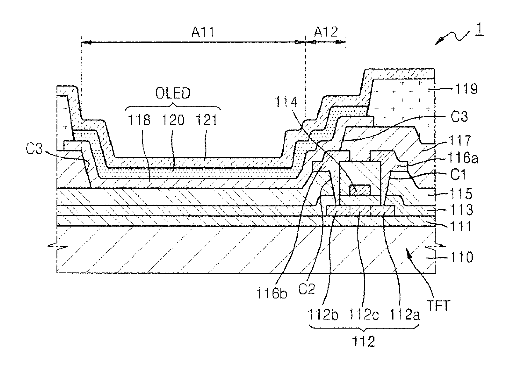
[0069]In contrast, in the organic light emitting display apparatus 1 the first electrode 118 and the drain electrode 116b are directly connected to each other without a via hole so that the emission area may be extended and an aperture ratio may be increased.

[0070]Hereinafter, an organic light emitting display apparatus will now be described with reference to FIG. 5.

second embodiment

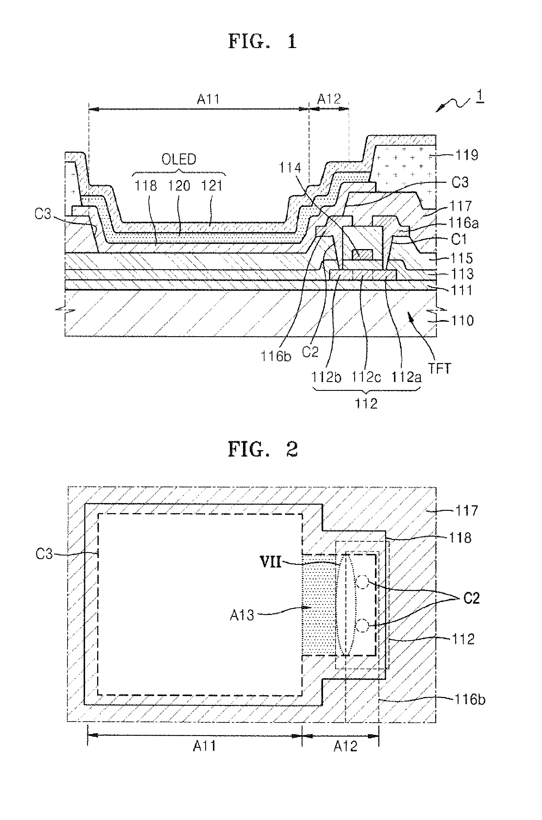
[0071]FIG. 5 is a planar view illustrating a relation between a third insulating layer and a first electrode of the organic light emitting display apparatus according to the present invention.

[0072]Referring to FIG. 5, a first region A21 and a second region A22 are formed as one opening C6 which is integrally connected to the third insulating layer 117-2. That is, a via hole to connect the first electrode 118-2 and a drain electrode 116b is not separately formed between the first region A21 and the second region A22 of the third insulating layer 117-2. Thus, compared to the aforementioned comparative example, the emission area of the second embodiment is extended (refer to A23-1).

[0073]The opening C6 formed in the second region A22 is not only formed in the drain electrode 116b of a TFT but also extends to and is formed in an outer portion of the drain electrode 116b (refer to A23-2 and A23-3).

[0074]In the organic light emitting display apparatus 2 of FIG. 4 according to the aforeme...

third embodiment

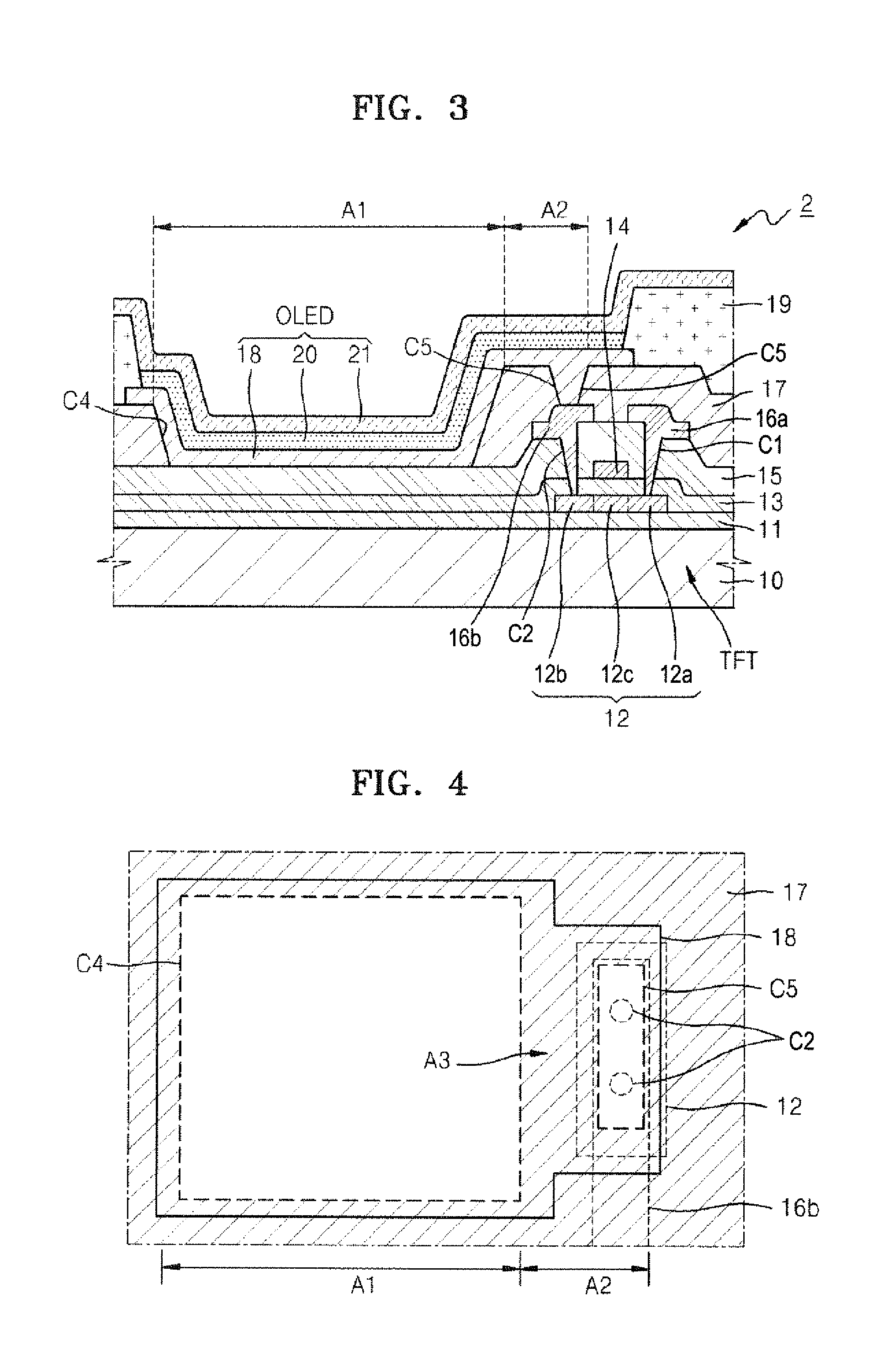
[0077]FIG. 6 is a planar view illustrating a relation between a third insulating layer and a first electrode of the organic light emitting display apparatus according to the present invention.

[0078]Referring to FIG. 6, a first region A31 and a second region A32 are formed as one opening C7 which is integrally connected to the third insulating layer 117-3. That is, a via hole to connect the first electrode 118-3 and a drain electrode 116b is not separately formed between the first region A31 and the second region A32 of the third insulating layer 117-3. Thus, compared to the aforementioned comparative example, the emission area of the third embodiment is extended (refer to A33).

[0079]However, in the present embodiment, the opening C7 formed in the second region A32 does not entirely expose the drain electrode 116b of a TFT, and non-openings NC in which the third insulating layer 117-3 exists are formed in a portion of the drain electrode 116b. The non-openings NC may be formed in a r...


PUM


Abstract

A substrate includes a thin film transistor (TFT) which includes an active layer, a gate electrode, a source electrode, and a drain electrode; a first insulating layer disposed between the active layer and the gate electrode; a second insulating layer disposed between the gate electrode and the source and drain electrodes; a third insulating layer disposed on the second insulating layer, and including a first region for opening the second insulating layer and a second region for opening one of the source and drain electrodes, the first region and the second region being integrally connected; and a first electrode connected to one of the source and drain electrodes, and disposed so as to cover the first region and the second region.

Description

CLAIM OF PRIORITY[0001]This application makes reference to, incorporates the same herein, and claims all benefits accruing under 35 U.S.C. §119 from an application earlier filed in the Korean Intellectual Property Office on the 5 Jan. 2012 and there duly assigned Serial No. 10-2012-0001551.BACKGROUND OF THE INVENTION[0002]1. Field of the Invention[0003]The present invention relates to a substrate including thin film transistors (TFTs), and an organic light emitting display apparatus including the substrate, and more particularly, to an active-matrix (AM) bottom emission type organic light emitting display apparatus.[0004]2. Description of the Related Art[0005]Recently, display apparatuses have been replaced with portable, thin flat panel display apparatuses. Among the flat panel display apparatuses, electroluminescent display apparatuses are self-emissive display apparatuses that display an image by using light generated by recombination of electrons and holes in an emission layer (...

Claims


Application Information

Patent Timeline
Patent Type & Authority Patents(United States)
IPC IPC(8): H01L27/32H01L29/786
CPCH01L27/124H01L27/1248H10K59/123H10K59/124H10K2102/3023
Inventor LEE, WON-KYUCHANG, YOUNG-JINJIN, SEONG-HYUN
Owner SAMSUNG DISPLAY CO LTD
Features
  • R&D
  • Intellectual Property
  • Life Sciences
  • Materials
  • Tech Scout
  • Unparalleled Data Quality
  • Higher Quality Content
  • 60% Fewer Hallucinations
Learn More