Device substrate
a technology of device substrates and substrates, applied in the field of device substrates, to achieve the effect of avoiding interference, shortening distance, and avoiding interferen
- Summary
- Abstract
- Description
- Claims
- Application Information
AI Technical Summary
Benefits of technology
Problems solved by technology
Method used
Image

Examples
Embodiment Construction
[0044]Hereinafter, an embodiment of the present invention will be described with reference to the accompanying drawings.
[0045]
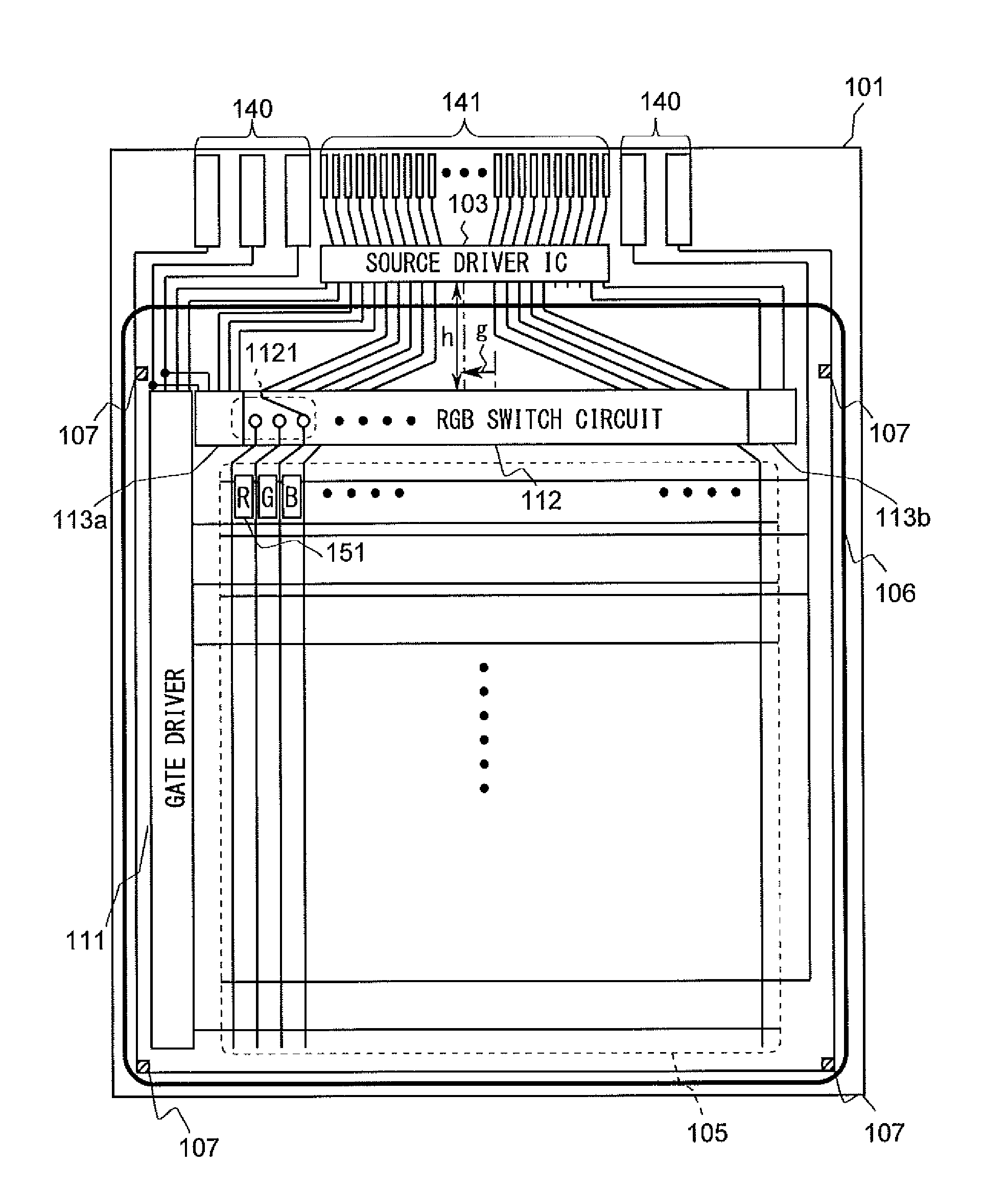
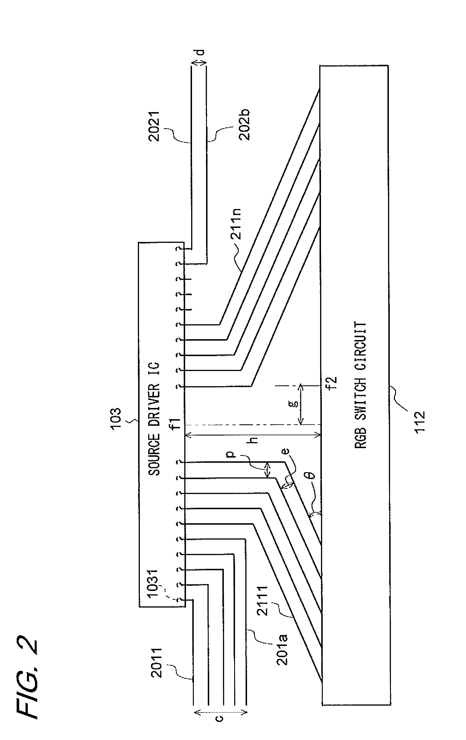
[0046]A liquid crystal panel, which is a display device according to an embodiment of the present invention, has almost the same configuration as conventional, except for features related to the position in which to arrange the source driver IC. Specifically, as with the external configuration of the conventional liquid crystal panel 900 shown in FIG. 4 and described earlier, this liquid crystal panel is configured by attaching an element-side substrate, which is a display device substrate, to an opposing-side substrate via a predetermined seal material in which the liquid crystal layer is enclosed between the substrates. In addition, the element-side substrate is connected to an FPC substrate to which video signals are externally transmitted, and the video signals are supplied through the FPC substrate to the source driver IC 103 provided on the element-side...
PUM
| Property | Measurement | Unit |
|---|---|---|
| angle | aaaaa | aaaaa |
| angles | aaaaa | aaaaa |
| distance | aaaaa | aaaaa |
Abstract
Description
Claims
Application Information
 - R&D
- Intellectual Property
- Life Sciences
- Materials
- Tech Scout
- Unparalleled Data Quality
- Higher Quality Content
- 60% Fewer Hallucinations
Browse by: Latest US Patents, China's latest patents, Technical Efficacy Thesaurus, Application Domain, Technology Topic, Popular Technical Reports.
© 2025 PatSnap. All rights reserved.Legal|Privacy policy|Modern Slavery Act Transparency Statement|Sitemap|About US| Contact US: help@patsnap.com