Pixel array

a pixel array and array technology, applied in the field of pixel arrays, can solve the problems of more severe color shift phenomenon or inadequate color saturation, side view image still has problems of blue-bias, green-bias or red-bias

Active Publication Date: 2015-02-03
AU OPTRONICS CORP
View PDF7 Cites 5 Cited by
  • Summary
  • Abstract
  • Description
  • Claims
  • Application Information

AI Technical Summary

Benefits of technology

[0008]The invention is directed to a pixel array, which is capable of mitigating a problem of an existing technique that a side view image has a color shift problem under different viewing angles compared to a front view image.
[0012]According to the above descriptions, the color shift problem of the side view image of various color pixel units can be mitigated by adjusting the extending directions of the slits of the pixel electrodes, the area ratios of the pixel electrodes, the voltage ratios of the pixel electrodes of the first color pixel unit, the second color pixel unit and the third color pixel unit and combinations thereof.

Problems solved by technology

Particularly, the color shift phenomenon or inadequate color saturation is more severe in a display image of a middle-low gray level.
Although the aforementioned methods for resolving the color shift phenomenon or inadequate color saturation can mitigate a problem of white-bias in case of a large viewing angle (side view), compared to a front view image, a side view image still has problems of blue-bias, green-bias or red-bias under different viewing angles.

Method used


Image

  • Pixel array
  • Pixel array
  • Pixel array

Examples


first embodiment

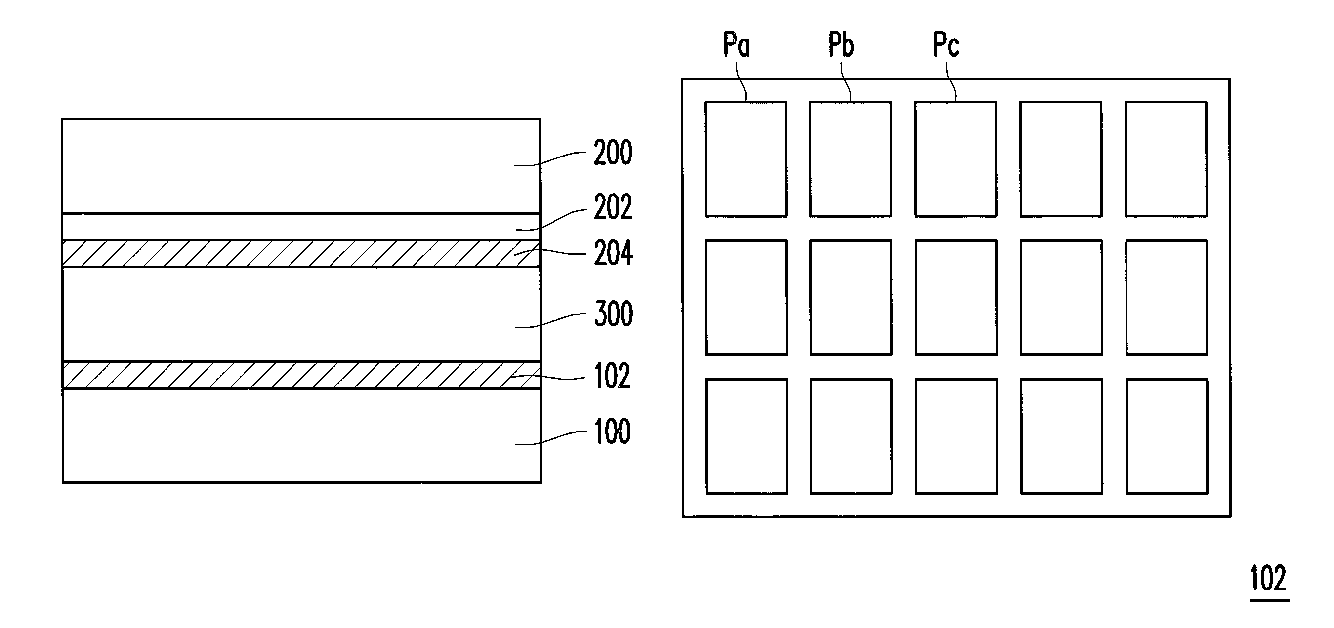
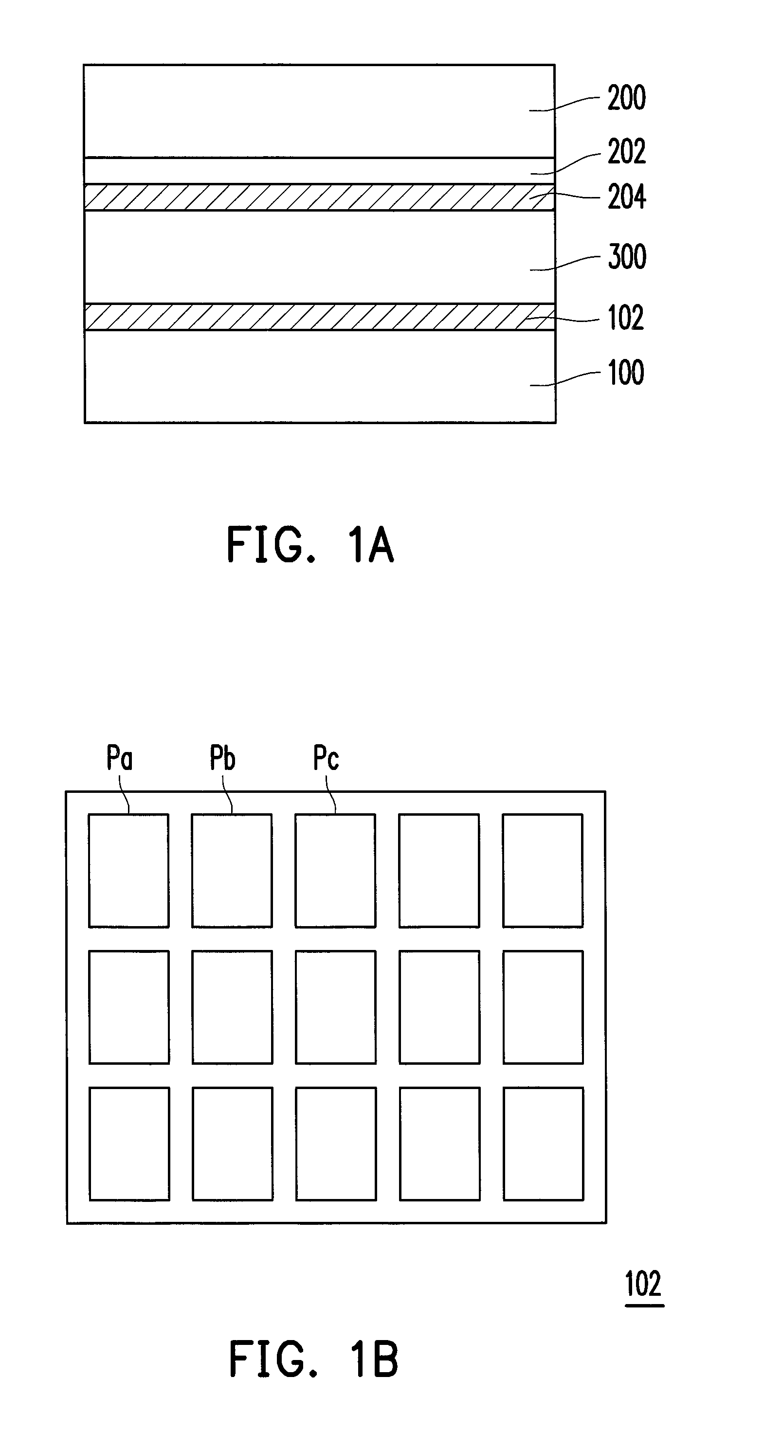
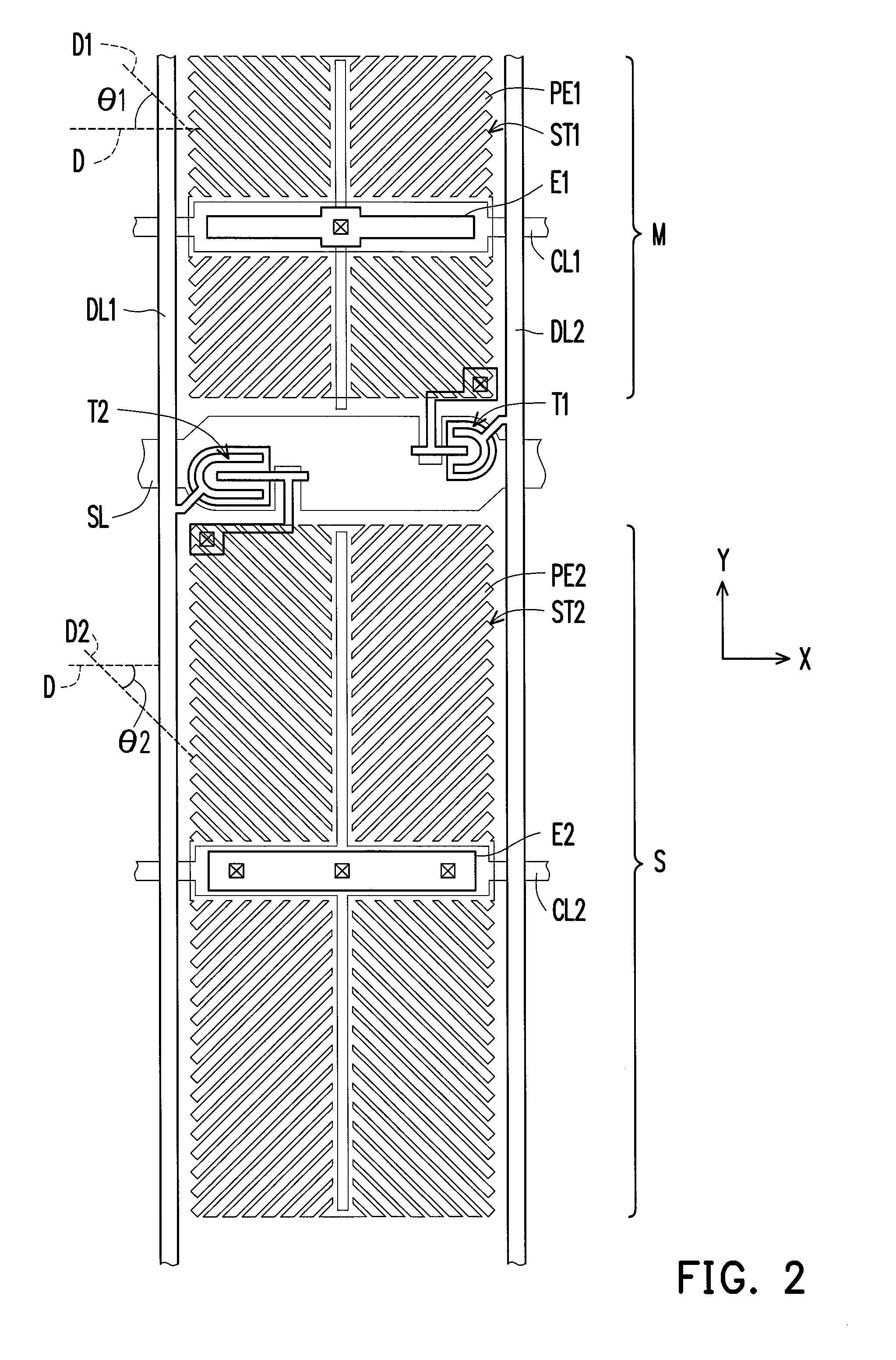
[0042]FIG. 2 is a schematic diagram of a pixel unit in a pixel array according to an embodiment of the invention. FIG. 3 is a schematic diagram of a pixel array according to an embodiment of the invention. A structure of each of the first, the second and the third color pixel units Pa, Pb and Pc is as that shown in FIG. 2, which includes a scan line SL, data lines DL1 and DL2, at least one active device T1 and T2 and a first pixel electrode PE1. Here, the first, the second and the third color pixel units Pa, Pb and Pc respectively further include a second pixel electrode PE2, capacitor electrode lines CL1 and CL2 and upper electrodes E1 and E2.

[0043]Here, the scan line SL and the data lines DL1 and DL2 are intersected, and an insulation layer is disposed between the scan line SL and the data lines DL1 and DL2. In other words, an extending direction of the scan line SL is not parallel to an extending direction of the data lines DL1 and DL2. Preferably, the extending direction of the ...

second embodiment

[0057]FIG. 5A is a schematic diagram of a pixel unit in a pixel array according to an embodiment of the invention. FIG. 5B is a schematic diagram of a pixel array according to an embodiment of the invention. A pixel unit structure of the present embodiment is similar to the pixel unit structure of FIG. 2, so that the same or similar devices are represented by the same or similar symbols, and details thereof are not repeated. Referring to FIG. 5A and FIG. 5B, structures of the first, the second and the third color pixel units Pa, Pb and Pc of the present embodiment are as that shown in FIG. 5A, which includes a scan line SL, a data line DL, an active device T and a pixel electrode PE.

[0058]Here, the scan line SL is intersected to the data line DL. The active device T can be a bottom gate type thin film transistor or a top gate type thin film transistor, which includes a gate, a channel, a source and a drain. The active device T is electrically connected to the scan line SL and the da...

third embodiment

[0066]FIG. 7 is a schematic diagram of a pixel array according to an embodiment of the invention. Referring to FIG. 7, the pixel array of FIG. 7 is similar to the pixel array of FIG. 3, so that the same or similar devices are represented by the same or similar symbols, and details thereof are not repeated. In the present embodiment, the pixel array includes the first, the second and the third color pixel units Pa, Pb, Pc, and structures thereof are as that shown in FIG. 2, so that the first, the second and the third color pixel units Pa, Pb, Pc respectively have the main pixel region M and the sub pixel region S.

[0067]A difference between the pixel array of the present embodiment and the pixel array of FIG. 3 is that the first acute angles θa-1, θb-1, θc-1 and the second acute angles θa-2, θb-2, θc-2 of the first color pixel unit Pa, the second color pixel unit Pb and the third color pixel unit Pc are all the same. However, area ratios and voltage ratios of the first pixel electrode...


PUM

PropertyMeasurementUnit
acute angle θcaaaaaaaaaa

Abstract

A pixel array includes a first color pixel unit, a second color pixel unit and a third pixel unit, and the first, second and third pixel units respectively include a scan line, a data line, an active device electrically connected to the scan line and the data line and a first pixel electrode electrically connected to the active device. The first pixel electrode has at least one first slit, and a first acute angle is formed between an extending direction of the first slit and an extending direction of the scan line. Any two of the first acute angle of the first color pixel unit, the first acute angle of the second color pixel unit, and the first acute angle of the third color pixel unit are different.

Description

CROSS-REFERENCE TO RELATED APPLICATION[0001]This application claims the priority benefits of Taiwan application serial no. 100141251, filed on Nov. 11, 2011, and Taiwan application serial no. 100146897, filed on Dec. 16, 2011. The entirety of each of the above-mentioned patent applications is hereby incorporated by reference herein and made a part of specification.BACKGROUND OF THE INVENTION[0002]1. Field of the Invention[0003]The invention relates to a pixel array. Particularly, the invention relates to a pixel array of a liquid crystal display (LCD) panel.[0004]2. Description of Related Art[0005]As liquid crystal displays (LCDs) are developed to have a large size, in order to resolve a viewing angle problem under a large size display specification, a wide viewing angle technique of a LCD panel has to be constantly developed. A multi-domain vertical alignment (MVA) LCD panel is a commonly used wide viewing angle technique.[0006]In the LCD panel, an alignment pattern is designed to ...

Claims


Application Information

Patent Timeline
Patent Type & Authority Patents(United States)
IPC IPC(8): G09G5/10G09G3/36G02F1/1337G02F1/139
CPCG02F1/133707G09G3/3648G02F1/133753G02F1/1393G09G2300/0447G09G3/3696
Inventor TIEN, KUN-CHENGWU, YU-CHINGWU, MING-HUEITING, TIEN-LUNLIAO, CHIEN-HUANGHSU, WEN-HAO
Owner AU OPTRONICS CORP
Why Eureka
Try Eureka