
Apparatus and method of fabricating alignment layer for liquid crystal display using a nano pattern mold

a technology of alignment layer and nano pattern mold, which is applied in the direction of surface layering apparatus, manufacturing tools, instruments, etc., can solve the problems of deterioration of contrast characteristics of liquid crystal displays, display defects, and increase black luminance , the effect of deterioration of contrast characteristics

Inactive Publication Date: 2015-02-03
LG DISPLAY CO LTD
View PDF6 Cites 0 Cited by
  • Summary
  • Abstract
  • Description
  • Claims
  • Application Information

AI Technical Summary

Benefits of technology

[0013]It is one object of the present invention to provide an apparatus and method for fabricating an alignment layer for liquid crystal displays, capable of shortening process time, preventing scratches of alignment layers and decreasing black luminance.

Problems solved by technology

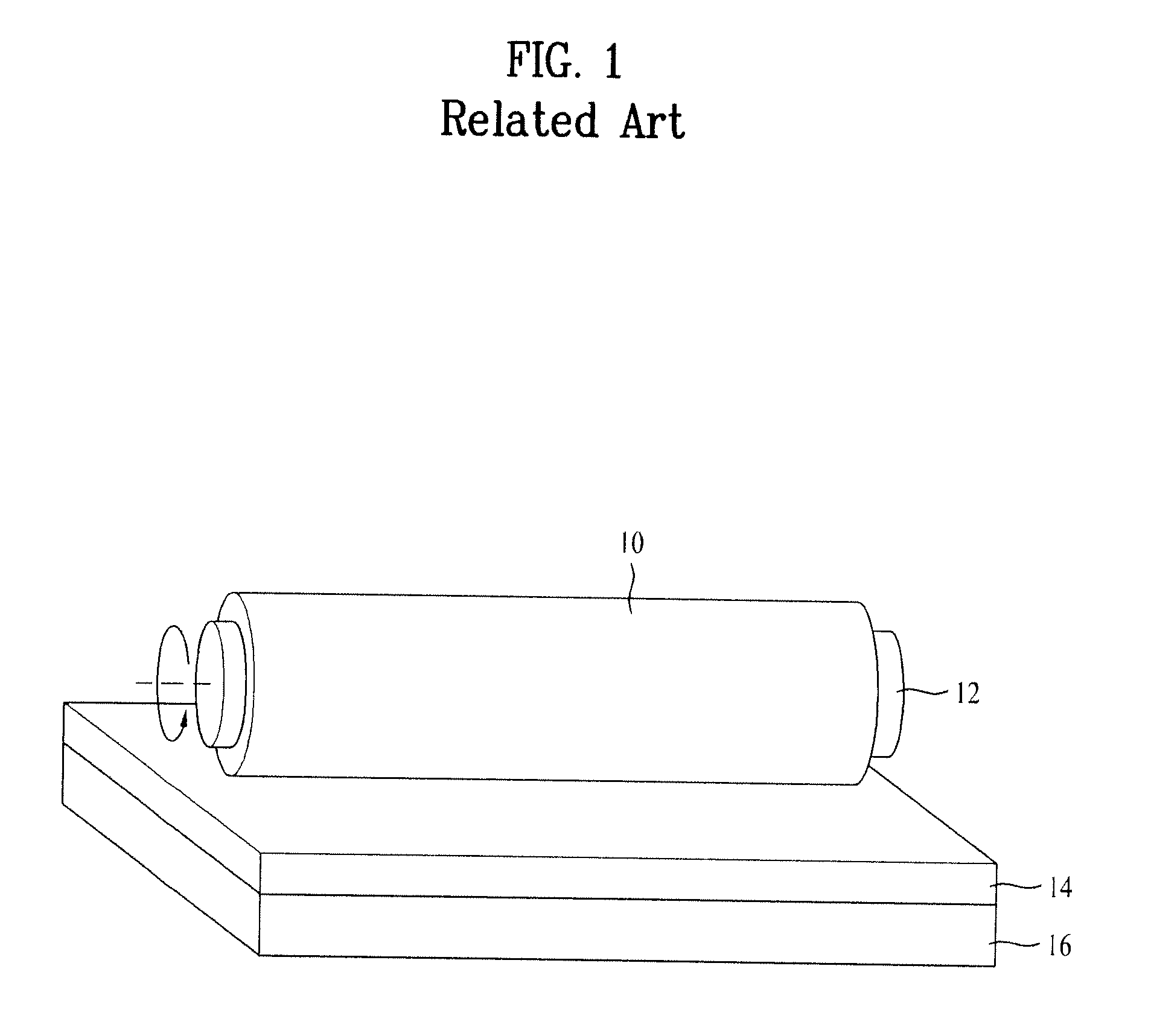
These foreign materials remain on the alignment layer 14, causing display defects, such as spots.
Meanwhile, the static electricity may cause breakage of thin films and thin film transistors.
This non-uniform alignment induces light leakage, increasing black luminance and deteriorating contrast characteristics of liquid crystal displays.
Furthermore, when such an alignment layer is formed to large-area panels, uniform control of the rubbing roller 12 becomes difficult, thus preventing realization of uniform alignment of liquid crystals.

Method used


Image

  • Apparatus and method of fabricating alignment layer for liquid crystal display using a nano pattern mold
  • Apparatus and method of fabricating alignment layer for liquid crystal display using a nano pattern mold
  • Apparatus and method of fabricating alignment layer for liquid crystal display using a nano pattern mold

Examples


Embodiment Construction

[0035]Hereinafter, preferred embodiments of the present invention will be described in detail with reference to the accompanying drawings.

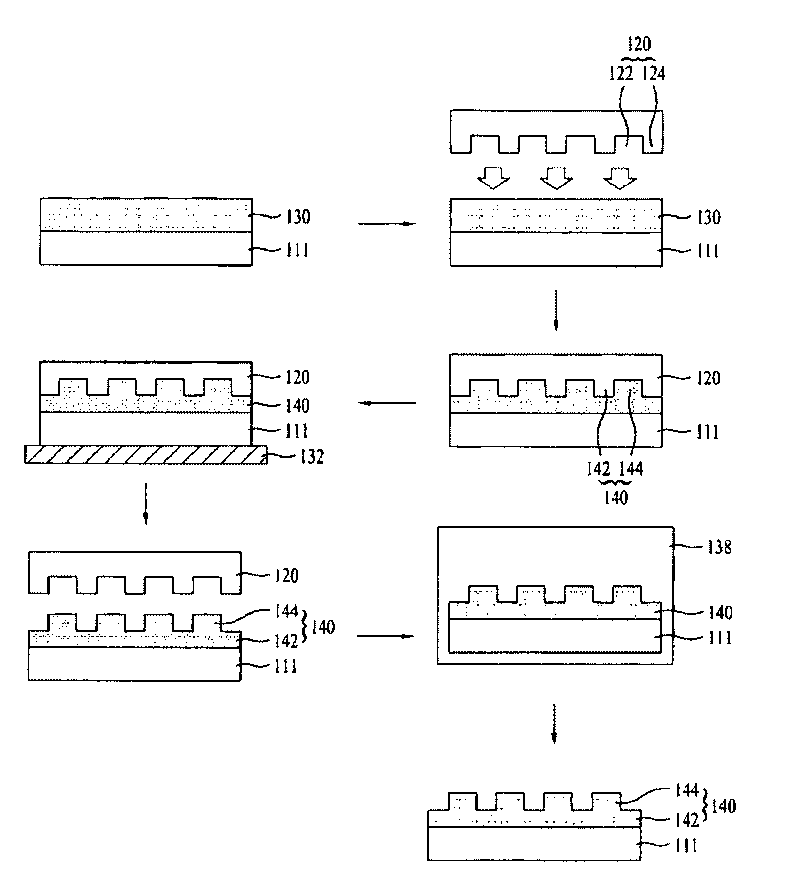
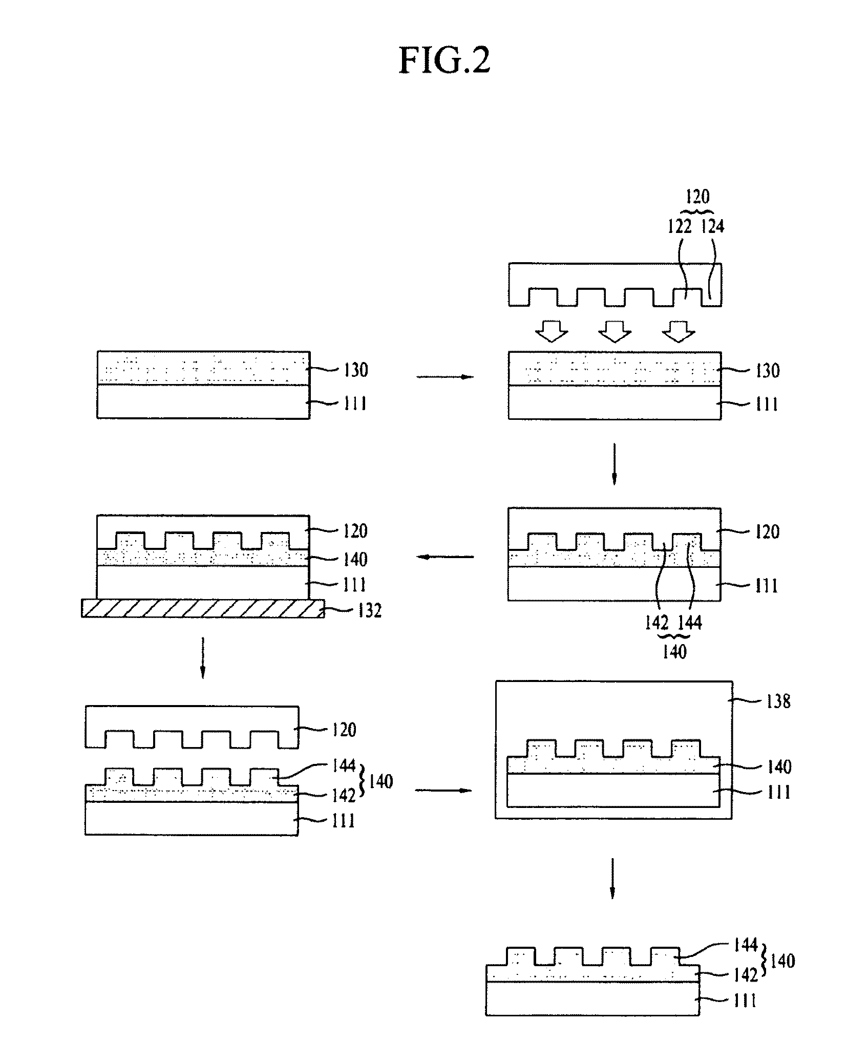
[0036]FIG. 2 is a flow chart illustrating a method for fabricating an alignment layer for liquid crystal displays according to one embodiment of the present invention. FIGS. 3A to 3G are perspective views illustrating a method for fabricating an alignment layer for liquid crystal displays according to the present invention in detail. The method for fabricating the alignment layer of the liquid crystal displays will be described in detail with reference to FIG. 2 and FIGS. 3A to 3F.

[0037]As shown in FIGS. 2 and 3A, an alignment agent 130 is coated to a substrate 111 by a method such as spin or spinless coating. For example, the alignment agent 130 is formed to a thickness of about 100 to 300 nm. In the case wherein the thickness of the alignment agent 130 is less than 100 nm, when a nano pattern mold 120 (which will be described in detail below) co...


PUM

PropertyMeasurementUnit
thicknessaaaaaaaaaa
depthaaaaaaaaaa
depthaaaaaaaaaa

Abstract

Disclosed are an apparatus and method for fabricating an alignment layer for liquid crystal displays, capable of shortening process time, preventing scratches of alignment layers and decreasing black luminance. The method includes coating an alignment agent on a substrate, arranging a nano pattern mold with a groove and a protrusion to contact the alignment agent, pre-curing the alignment agent, separating the nano pattern mold from the alignment agent, and hard-curing the alignment agent separated from the nano pattern mold to form an alignment layer.

Description

[0001]This application claims the benefit of Korean Patent Application No. 2009-0079137, filed on Aug. 26, 2009, which is hereby incorporated by reference for all purposes as if fully set forth herein.BACKGROUND OF THE INVENTION[0002]1. Field of the Invention[0003]The present invention relates to an apparatus and method for fabricating an alignment layer for liquid crystal displays, capable of shortening process time, and preventing scratches of alignment layers and decreasing black luminance.[0004]2. Discussion of the Related Art[0005]In general, liquid crystal displays control light transmission of liquid crystals using an electric field to display an image. Such a liquid crystal display comprises a thin film transistor substrate and a color filter substrate, which face each other; and liquid crystals interposed therebetween.[0006]The thin film transistor substrate comprises a gate line and a data line which intersect each other, a thin film transistor arranged at the intersection...

Claims


Application Information

Patent Timeline
Patent Type & Authority Patents(United States)
IPC IPC(8): G02F1/1337G02F1/13
CPCG02F1/13378G02F2001/133765G02F2202/36G02F1/133765
Inventor AHN, HAN-JINHWANG, HAN-SHIN
Owner LG DISPLAY CO LTD
Learn More