Transparent conductive laminate, touch panel and liquid crystal display unit with touch panel

a technology of transparent conductive laminate and touch panel, which is applied in the direction of thin material processing, instruments, chemistry apparatus and processes, etc., can solve the problems of insufficient adhesion reliability, difficult to distinguish display, and difficulty in removing liquid crystal display light by 14 wavelength retardation film, etc., to reduce the visibility of liquid crystal display, prevent scratches of polymer film, and enhance cohesion

Inactive Publication Date: 2006-01-19
TEIJIN LTD
View PDF22 Cites 61 Cited by
  • Summary
  • Abstract
  • Description
  • Claims
  • Application Information

AI Technical Summary

Benefits of technology

[0086] In order to control wavelength dispersion of retardation, for example, a compound layer (for example, a polymer liquid crystal layer) exhibiting retardation may be formed on the polymer films A, B, or a compound such as low molecular liquid crystals may be included in the polymer films A, B, in a range which does not impede the effect of the invention.
[0087] The polymer film B may be made of the same material as the polymer film A. The film thickness and manufacturing process may also be the same as for the polymer film A. <Light-Scattering Layer>
[0088] A light-scattering layer is formed on one side of the polymer film A. The light-scattering layer has the function of scattering light, but it may also sometimes function to enhance the cohesion between the polymer film A and the polymer film B or the polymer film A and the polarizing plate, or to act as a layer with the function of preventing scratches of the polymer film A during manufacturing process of the transparent conductive laminate. The light-scattering layer alone has a haze value of 0.2-1.4%, and preferably 0.3-1%. The haze value of the light-scattering layer alone may be determined as the difference in the haze value before formation and after formation of the light-scattering layer on the polymer film A. If the haze value of the light-scattering layer alone is less than 0.2%, red-green stripes become distinguishable due to film thickness deviation, thus reducing the visibility of the liquid crystal display. The slip property is also impaired, thereby eliminating the effect of preventing scratches of the polymer film A during manufacturing process of the transparent conductive laminated. A haze value of greater than 1.4% will also tend to impair the visibility of the liquid crystal display.
[0089] The thickness of the light-scattering layer is preferably 1-5 μm and more preferably 1-4 μm. When the surface contains unevenness and is not substantially flat, the thickness is defined as the average value of measuring the film thickness at more than 10 arbitrary points.
[0090] The light-scattering layer scatters light inside and / or on the surface of the layer. The method of forming the light-scattering layer on the surface of the polymer film A may be, for example, a method of forming a polymer layer containing fine particles, or a method of producing fine-unevenness on the surface during forming a polymer layer containing no fine particles. In the former method, light scattering occurs inside the light-scattering layer due to the use of fine particles that have a different refractive index than the polymer. By using particles having a larger mean diameter than the thickness of the polymer layer, light scattering will occur on the surface regardless of the refractive index of the fine particles, because fine unevenness will be produced on the surface. In the latter method, unevenness may be formed by contacting an emboss roll or the like with the surface of the polymer layer during forming the polymer layer.
[0091] The light-scattering layer will have unevenness except in the case of utilizing only light scattering inside the light-scattering layer, and as surface texture parameter, a center line average roughness (Ra) is preferably in the range of 0.005-0.04 μm.

Problems solved by technology

Consequently, noise light (reflected light from the touch panel section) also enters the eye simultaneously with the image recognition light (for example, light from the liquid crystal display), thus rendering the display more difficult to distinguish.
The touch panel is effective for reducing reflected light from the touch panel section, but coloration of light from the liquid crystal display by the ¼ wavelength retardation film has been a problem.
However, it has been found that lack of a protective layer on a side opposite to the transparent conductive layer-formed side of the retardation film can sometimes create problems during actual manufacturing, such as scratching of the retardation film during the process of forming the transparent conductive layer or the processes of making up the touch panel, or can lead to insufficient reliability of adhesion when the retardation film is attached to the polarizing plate.
However, it has become apparent that when a layer, which performs a function of improving adhesion with the polarizing plate as well as a function of preventing damage during the various making up processes, is formed on the polarizing plate lamination side of the retardation film, red-green stripes become distinguishable due to film thickness deviation of the layer and thus reduce the visibility of the liquid crystal display.
This method is effective for eliminating red-green stripes, but because center line average roughness is too large, the haze is increased and the visibility of the liquid crystal is thus impaired.

Method used


Image

  • Transparent conductive laminate, touch panel and liquid crystal display unit with touch panel
  • Transparent conductive laminate, touch panel and liquid crystal display unit with touch panel
  • Transparent conductive laminate, touch panel and liquid crystal display unit with touch panel

Examples


example 2

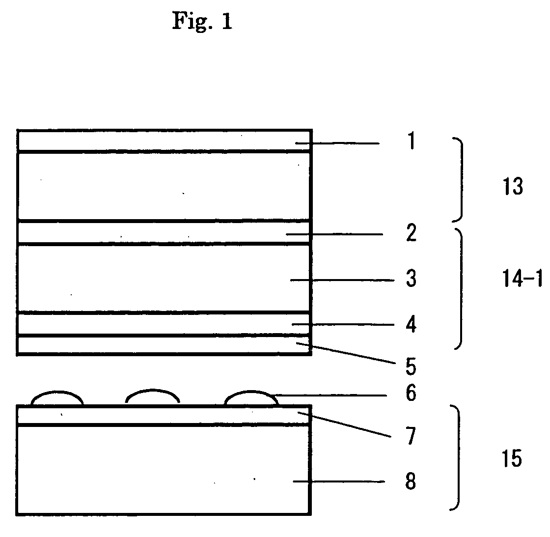
[0168] An approximately 2 μm-thick light-scattering layer (2) was formed on one side of the retardation film (3) of Example 1 in the same manner as Example 1. The haze value of the light-scattering layer alone was 0.5%. An approximately 2 μm-thick cured resin layer (4) was then formed on the side of the retardation film (3) opposite to the side on which the light-scattering layer was formed, in the same manner as Example 1.

[0169] Next, tetrabutoxy titanate (“B-4” by Nihon Soda) was diluted with a mixed solvent of ligroin (special grade product by Wako Pure Chemical Industries) and butanol (special grade product by Wako Pure Chemical Industries) to prepare coating solution D.

[0170]γ-Glycidoxypropyltrimethoxysilane (“KBM403” by Shin-Etsu Chemical Co., Ltd.) and methyltrimethoxysilane (“KBM13” by Shin-Etsu Chemical Co., Ltd.) were mixed in a molar ratio of 1:1 and hydrolysis of the silanes was carried out by a publicly-known method with aqueous acetic acid (pH=3.0) to obtain silane h...

example 4

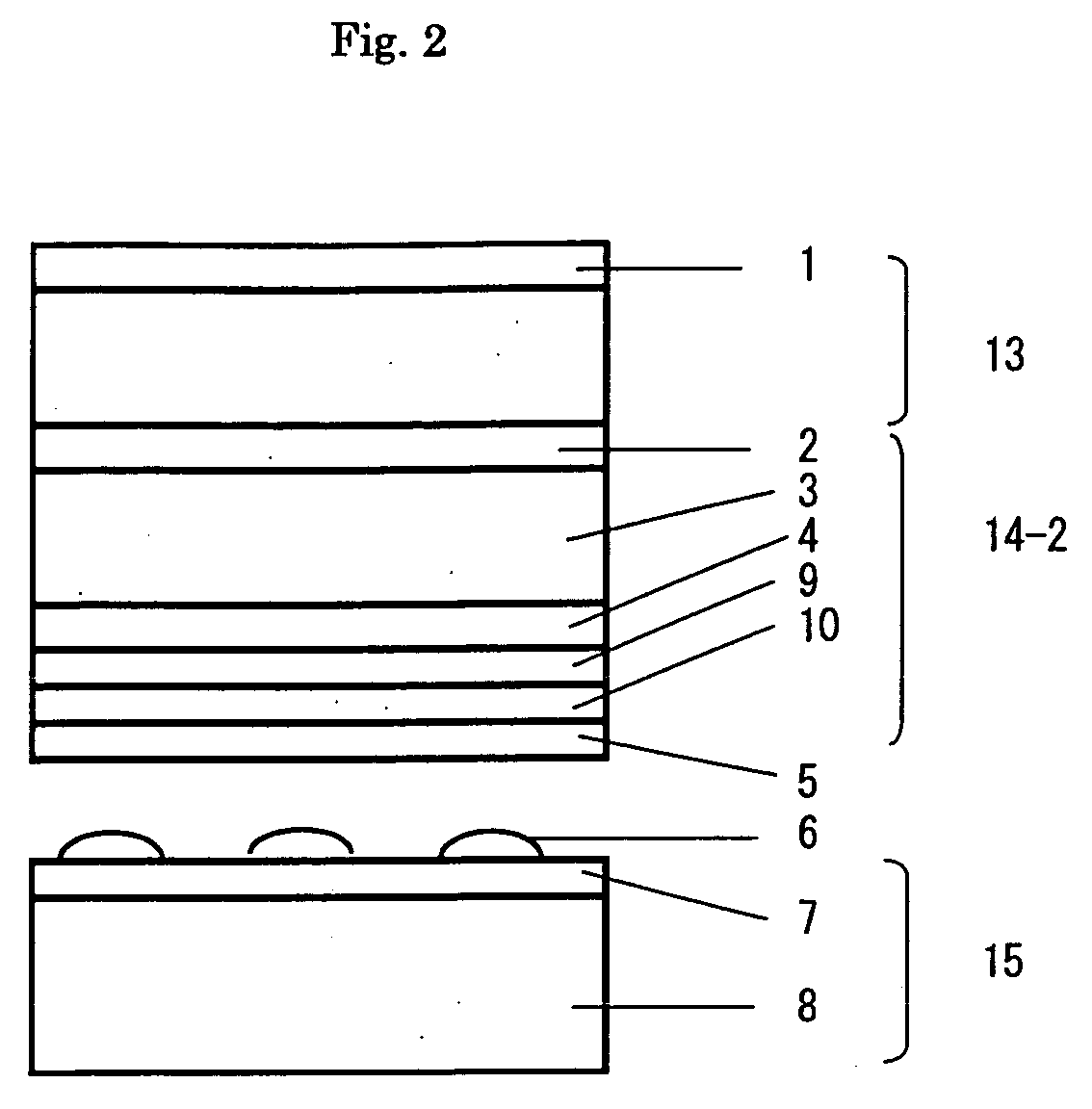
[0181] Coating solution G was prepared comprising 100 parts by weight of urethane acrylate, 7 parts by weight of a photoinitiator (IRGACURE 184, product of Ciba-Geigy), 135 parts by weight of 1-methoxy-2-propanol as a diluent and 135 parts by weight of isopropanol. To the coating solution G there were then added silicone crosslinked fine particles with a mean diameter of about 3 μm (TOSPEARL 130, product of GE-Toshiba Silicones) as fine particles A, at 0.2 part by weight to 100 parts by weight of the resin component, to obtain coating solution H. Separately, there were added to the coating solution G the silicone crosslinked fine particles with a mean particle size of about 3 μm (TOSPEARL 130, product of GE-Toshiba Silicones) as fine particles A at 0.7 part by weight to 100 parts by weight of the resin component, and MgF2 superfine particles as superfine particles B at 5 parts by weight to 100 parts by weight of the resin component, to obtain coating solution I.

[0182] Coating solut...


PUM

PropertyMeasurementUnit
Tgaaaaaaaaaa
Tgaaaaaaaaaa
Tgaaaaaaaaaa

Abstract

The transparent conductive laminate of the invention is a laminate comprising a film made of a polymer with a photoelastic constant of no greater than 70×10−12 Pa−1, a light-scattering layer with a haze value in the range of 0.2-1.4% formed on one side thereof, and a transparent conductive layer formed on the other side thereof, wherein the laminate exhibits an overall retardation of λ / 4. By using the laminate it is possible to provide touch panels with reduced light reflection, no coloration, excellent visibility and high reliability for outdoor use, as well as touch panel-equipped liquid crystal displays employing them.

Description

FIELD OF THE INVENTION [0001] The present invention relates to a transparent conductive laminate. More specifically, it relates to a transparent conductive laminate that is particularly suitable for use in touch panels and touch panel-equipped liquid crystal displays. BACKGROUND ART [0002] Recently, the wide employment of information-processing equipment, on which a liquid crystal display for displaying information and a touch panel (called a touch screen, a transparent membrane switch) for inputting information were mounted, began. Most of the touch panels are resistance film type ones. The resistance film type touch panels are fabricated by setting two transparent electrode substrates (a movable electrode substrate and a fixed electrode substrate) having transparent conductive layers formed thereon, respectively, facing each other at a distance of 10 to 100 μm. In order to maintain insulation between the movable electrode substrate and fixed electrode substrate in the absence of e...

Claims


Application Information

Patent Timeline
Patent Type & Authority Applications(United States)
IPC IPC(8): C09K19/00G02F1/133
CPCG02F1/13338Y10T428/10Y10T428/105C09K2323/00C09K2323/035B32B7/12B32B2307/42C08J5/18G02B5/3033G02F1/133528
Inventor MIKOSHIBA, HITOSHIITO, HARUHIKOSHIROISHI, ISAO
Owner TEIJIN LTD
Why Eureka
Try Eureka