Tertiary amine compounds, organic semiconductor devices using the same and organic electroluminescence devices using the same

a technology of organic semiconductor and tertiary amine, which is applied in the direction of thermoelectric devices, organic semiconductor devices, discharge tube luminescnet screens, etc., can solve the problems of affecting the overall electrical conduction and voltage response of the device, the deterioration of the device performance, and the drastic increase in the consumption of power, so as to improve the overall electrical conduction and voltage response, the effect of high durability

Active Publication Date: 2006-07-06
NISHIO TETABUYA
View PDF1 Cites 53 Cited by
  • Summary
  • Abstract
  • Description
  • Claims
  • Application Information

AI Technical Summary

Benefits of technology

[0023] According to the invention, it is possible to obtain a tertiary amine compound having a high packing property, excellent in overall electrical conduction and voltage response because hopping conduction occurs efficiently, and having high durability and time-dependent stability.
[0024] In add

Problems solved by technology

Polythiophene is sparingly soluble in a solution and in addition, owing to heating at high temperature while using a solution of a strong acid such as hydrochloric acid, it tends to cause corrosion of electrodes or deterioration of device performance.
It is therefore inferior in mass productivity and device reliability.
Secondly, as a low molecule type, an organic semiconductor device using pentacene is under investigation.
It has, however, been generally pointed out as a problem that in this device, an excess voltage must be applied to a gate electrode because a current running between a source electrode and a drain electrode is inevitably small, which results in a drastic increase in a consumed power and in addition, tends to cause dielectric breakdown of an organic film.
It burdens an external IC and in addition, makes circuit design difficult, which leads to a cost increase of the IC and deterioration in mass productivity.
Also from the viewpoint of performance, the device becomes unstable and has reduced reliability.
As a further problem which is expected to occur, the external IC will require a high level and complex circuit design in order to overcome the excessive current flow.
The semiconductor layer formed using it has a low strength, which lowers the reliability of the device.
As described above, low molecular weight compounds (such as pentacene) used so far for organic semiconductor devices have a problem that a current hysteresis relative to a drive voltage is large.
They also have a problem in time-dependent stability, and reliability against impact.
Smectic liquid crystal

Method used


Image

  • Tertiary amine compounds, organic semiconductor devices using the same and organic electroluminescence devices using the same
  • Tertiary amine compounds, organic semiconductor devices using the same and organic electroluminescence devices using the same
  • Tertiary amine compounds, organic semiconductor devices using the same and organic electroluminescence devices using the same

Examples


synthesis example 1

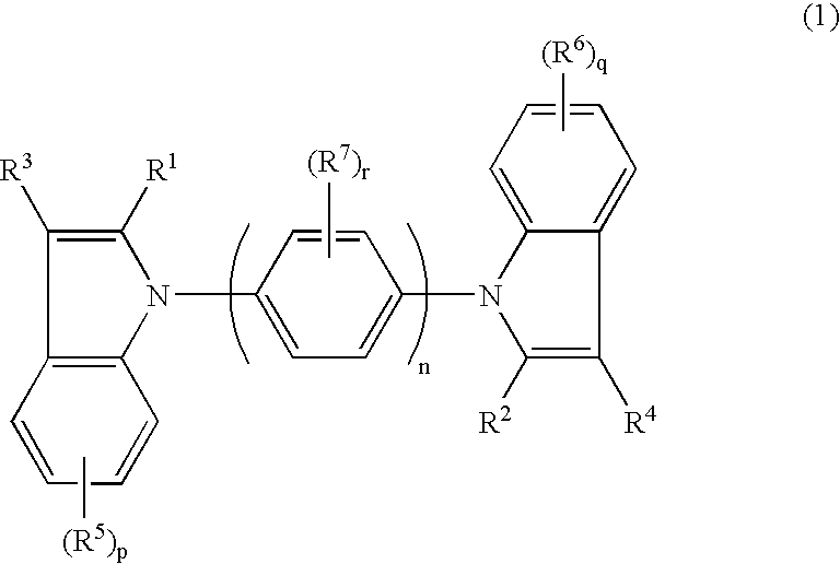
[0314] In 50 mL of dehydrated xylene were dissolved 0.04 g of palladium acetate and 0.12 g of tri-t-butylphosphine. To the resulting solution were added 0.90 g of 4,4-dibromobiphenyl, 1.40 g of 2-(2-naphthyl)indole and 0.65 g of sodium-t-butoxide, followed by heating under reflux at 125° C. for 24 hours in a nitrogen atmosphere. Chloroform and water were added to the reaction mixture and the resulting mixture was filtered. After the organic layer thus extracted was dried over magnesium sulfate, the solvent was distilled off under reduced pressure to give 0.70 g of a desired compound represented by the formula (142) in the crude form. The resulting compound was purified by column chromatography using a 1:1 chloroform and n-hexane mixture, followed by recrystallization from methanol to give 0.51 g of the desired compound represented by the formula (142). Nuclear magnetic resonance [1H-NMR] (solvent: CDCl3, internal standard: tetramethylsilane) and infrared absorption spectrum ([IR] (K...

synthesis example 2

[0316] In 50 mL of dehydrated xylene were dissolved 0.04 g of palladium acetate and 0.12 g of tri-t-butylphosphine. To the resulting solution were added 0.90 g of 4,4-dibromobiphenyl, 1.40 g of 2-(1-naphthyl)indole and 0.65 g of sodium-t-butoxide, followed by heating under reflux at 130° C. for 32 hours in a nitrogen atmosphere. Chloroform and water were added to the reaction mixture and the resulting mixture was filtered. After the organic layer thus extracted was dried over magnesium sulfate, the solvent was distilled off under reduced pressure to give 0.74 g of a desired compound represented by the formula (143) in the crude form. The resulting crude compound was purified by column chromatography using a 1:1 chloroform and n-hexane mixture, followed by recrystallization from methanol to give 0.57 g of the desired compound represented by the formula (143). Nuclear magnetic resonance [1H-NMR] (solvent: CDCl3, internal standard: tetramethylsilane) and infrared absorption spectrum ([...

synthesis example 3

[0317] In 50 mL of dehydrated xylene were dissolved 0.04 g of palladium acetate and 0.12 g of tri-t-butylphosphine. To the resulting solution were added 0.90 g of 4,4-dibromobiphenyl, 1.11 g of 2-phenylindole and 0.65 g of sodium-t-butoxide, followed by heating under reflux at 120° C. for 20 hours in a nitrogen atmosphere. Chloroform and water were added to the reaction mixture and the resulting mixture was filtered. After the organic layer was extracted and dried over magnesium sulfate, the solvent was distilled off under reduced pressure to give 0.62 g of a desired compound represented by the formula (144) in the crude form. The resulting crude compound was purified by column chromatography using a 1:1 chloroform and n-hexane mixture, followed by recrystallization from methanol to give 0.44 g of the desired compound represented by the formula (144). Nuclear magnetic resonance [1H-NMR] (solvent: CDCl3, internal standard: tetramethylsilane) and infrared absorption spectrum ([IR] (KB...


PUM


Abstract

An object of the present invention is to provide an organic semiconductor device comprising a semiconductor layer containing a compound with improved cohesive force, controllable molecular orientation, high packing property, high overall electrical conduction, high durability and high time-dependent stability. An organic semiconductor device comprising a substrate, a gate electrode, source and drain electrodes, and a semiconductor layer, wherein the semiconductor layer contains a tertiary amine compound represented by the formula (1) is provided.

Description

BACKGROUND OF THE INVENTION [0001] 1. Field of the Invention [0002] The present invention relates to a tertiary amine compound, and an organic semiconductor device and organic electroluminescence device using the compound. [0003] 2. Description of Related Art [0004] Organic semiconductor devices typically have a gate electrode, an insulating layer stacked on / above the gate electrode, a source electrode and a drain electrode formed on / above the insulating layer, and a semiconductor layer of an organic compound interposed between the source electrode and drain electrode. The semiconductor layer is formed by the vapor deposition method, application method, drop encapsulation method, vacuum encapsulation method or the like. Organic semiconductor materials suited for respective film forming methods and excellent in current voltage efficiency and length of life are under investigation. Owing to ease of the formation of a semiconductor layer, organic semiconductor devices have advantages s...

Claims


Application Information

Patent Timeline
IPC IPC(8): H01L29/08H01J1/62H01L35/24C07D403/02
CPCC07D209/08C07D401/04C07D487/04H01L51/0052H01L51/0067H01L51/0068H01L51/007H01L51/0072H01L51/0081H01L51/0085H01L51/0545H01L51/5012H01L51/5048H01L51/5088H01L51/5092H01L2251/308H10K85/615H10K85/6565H10K85/654H10K85/655H10K85/324H10K85/342H10K85/6572H10K10/466H10K50/14H10K50/17H10K50/171H10K50/11H10K2102/103
Inventor NISHIO, TETSUYA
Owner NISHIO TETABUYA
Why Eureka
Try Eureka