

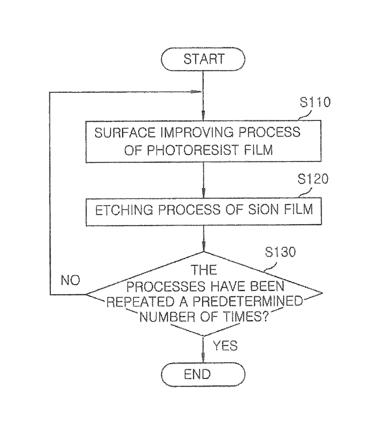
Plasma processing method
a processing method and technology of resist film, applied in the direction of electrical discharge tubes, decorative arts, electrical apparatus, etc., can solve the problems of etching rough achieve the effects of improving the surface of resist film, preventing etching, and good etching shap
- Summary
- Abstract
- Description
- Claims
- Application Information
AI Technical Summary
Benefits of technology
Problems solved by technology
Method used
Image

Examples
Embodiment Construction
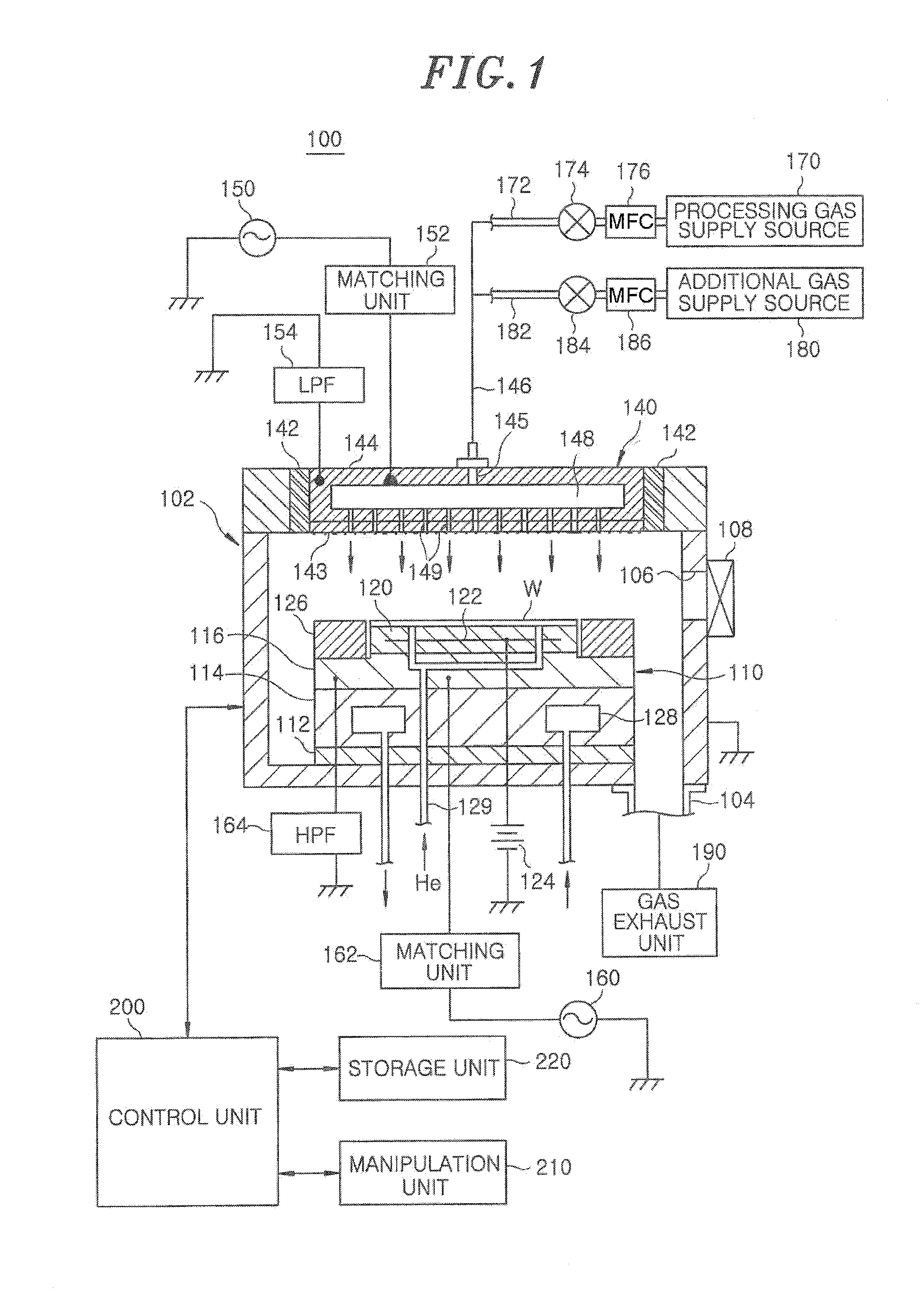
[0033]Hereinafter, an embodiment of the present invention will be described with reference to the accompanying drawings. In the present specification and the drawings, like reference numerals refer to like elements having substantially the same functions, and redundant description thereof will be omitted. In the present specification, 1 mTorr is (10−3×101325 / 760) Pa, and 1 sccm is (10−6 / 60) m3 / sec.
[0034](Configuration Example of Plasma Processing Apparatus)
[0035]First, a configuration example of a plasma processing apparatus to which a plasma processing method in accordance with an embodiment of the present invention is applied will be described. FIG. 1 is a cross sectional view showing a schematic configuration of a plasma processing apparatus 100 of the present embodiment. Here, a capacitive coupled plasma processing apparatus having a parallel plate type electrode structure will be described as an example.
[0036]As shown in FIG. 1, the plasma processing apparatus 100 includes a pr...
PUM
| Property | Measurement | Unit |
|---|---|---|
| frequency | aaaaa | aaaaa |
| frequency | aaaaa | aaaaa |
| frequency | aaaaa | aaaaa |
Abstract
Description
Claims
Application Information