Power semiconductor device and method of fabricating the same

a technology of power semiconductors and semiconductor devices, applied in the direction of semiconductor devices, basic electric elements, electrical equipment, etc., can solve the problem of easy breakage of devices, and achieve the effect of increasing current density and improving short circuit immunity

Inactive Publication Date: 2015-03-17
SAMSUNG ELECTRO MECHANICS CO LTD
View PDF8 Cites 0 Cited by
  • Summary
  • Abstract
  • Description
  • Claims
  • Application Information

AI Technical Summary

Benefits of technology

[0029]An aspect of the present invention provides a power semiconductor device having a gate insulating film of an immunity improving part having a thickness less than that of a gate of a current increasing unit, in order to simultaneously develop and improve short circuit immunity and an increase in current density of the power semiconductor device having a trade-off relationship to each other.

Problems solved by technology

However, due to structural limitations of the MOSFET, a bipolar transistor, a thyristor, gate turn-off thyristors (GTOs), and the like have been used in technical fields requiring high voltages.
However, in accordance with miniaturization of the device, in the case in which the magnitude of the voltage is increased, latch-up is generated due to a structure of the device, such that the device may easily break down.

Method used


Image

  • Power semiconductor device and method of fabricating the same
  • Power semiconductor device and method of fabricating the same
  • Power semiconductor device and method of fabricating the same

Examples


Embodiment Construction

[0055]Hereinafter, embodiments of the present invention will be described in detail with reference to the accompanying drawings. The invention may, however, be embodied in many different forms and should not be construed as being limited to the embodiments set forth herein.

[0056]Rather, these embodiments are provided so that this disclosure will be thorough and complete, and will fully convey the scope of the invention to those skilled in the art.

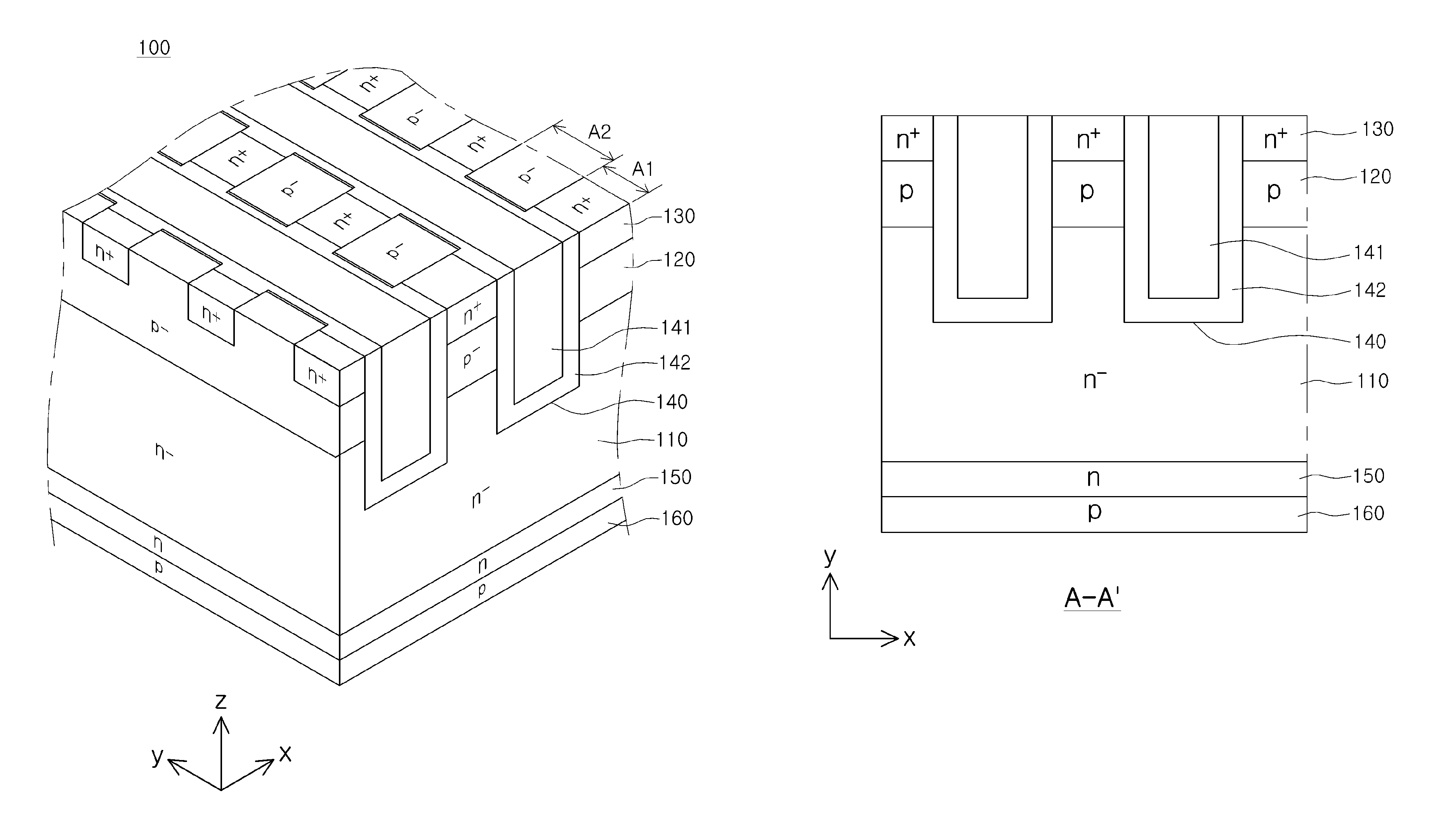
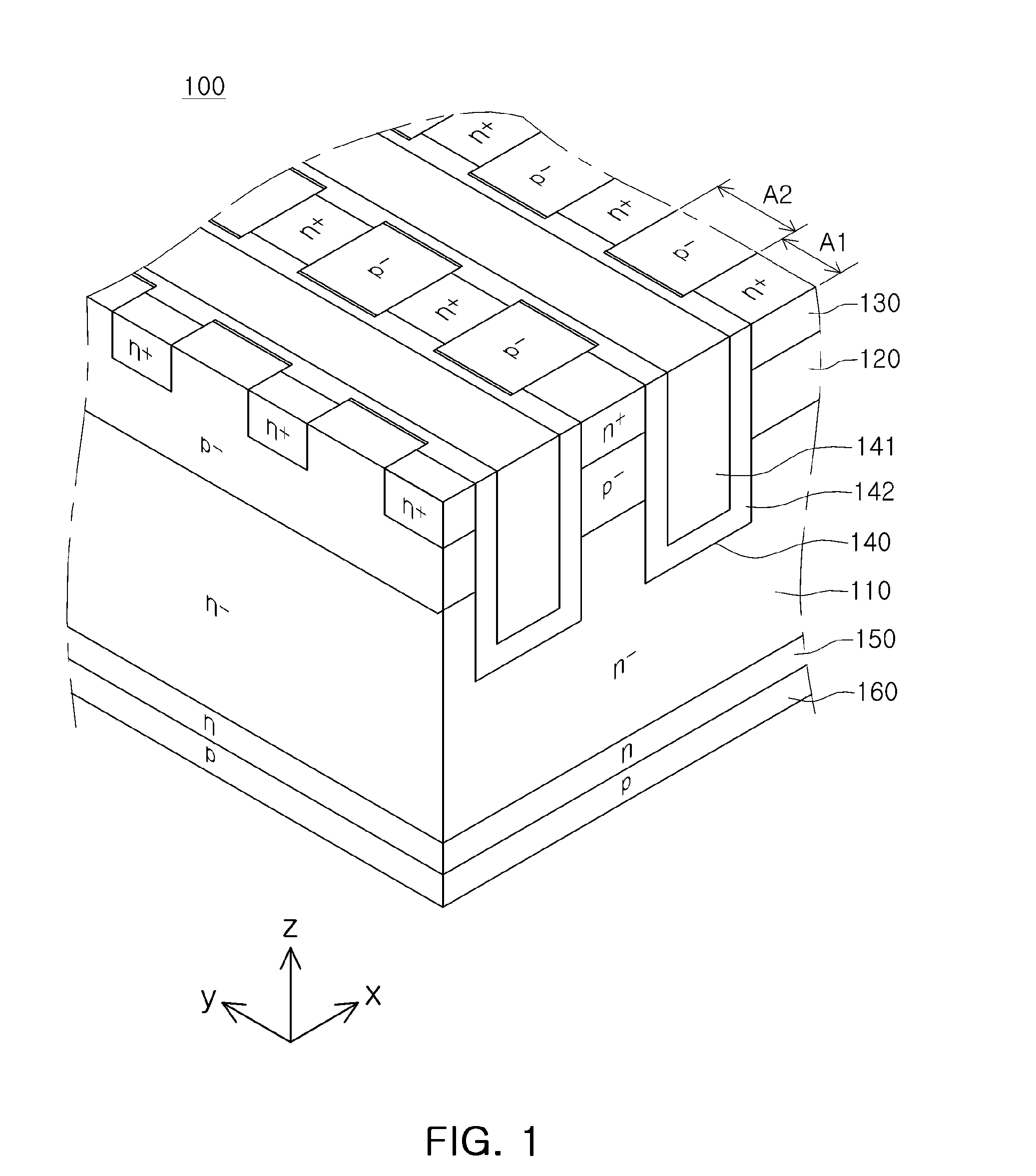
[0057]A power switch may be implemented by any one of a power MOSFET, an IGBT, several forms of thyristors, and those similar to the above-mentioned things. Most new technologies disclosed in the present invention will be described based on the IGBT. However, several embodiments of the present invention disclosed in the specification are not limited to the IGBT, but may be generally applied to different forms of power switch technologies including the power MOSFET and the several forms of thyristor, in addition to a diode, for example. Furt...


PUM


Abstract

There is provided a power semiconductor device, including a plurality of trench gates formed to be spaced apart from each other by a predetermined distance, a current increasing part formed between the trench gates and including a first conductivity-type emitter layer and a gate oxide formed on a surface of the trench gate, and an immunity improving part formed between the trench gates and including a second conductivity-type body layer, a preventing film formed on the surface of the trench gate, and a gate oxide having a thickness less than that the gate oxide of the current increasing part.

Description

CROSS-REFERENCE TO RELATED APPLICATIONS[0001]This application claims the priority of Korean Patent Application No. 10-2013-0034668 filed on Mar. 29, 2013, in the Korean Intellectual Property Office, the disclosure of which is incorporated herein by reference.BACKGROUND OF THE INVENTION[0002]1. Field of the Invention[0003]The present invention relates to a power semiconductor device and a method of fabricating the same.[0004]2. Description of the Related Art[0005]An insulated gate bipolar transistor (IGBT) refers to a transistor in which a gate is manufactured using a metal oxide semiconductor (MOS) and a p-type collector layer is formed on a rear surface to thereby have bipolarity.[0006]Since a power metal oxide semiconductor field effect transistor (MOSFET) according to the related art has been developed, the MOSFET has been used in a field requiring fast switching characteristics.[0007]However, due to structural limitations of the MOSFET, a bipolar transistor, a thyristor, gate tu...

Claims


Application Information

Patent Timeline
Patent Type & Authority Patents(United States)
IPC IPC(8): H01L29/66H01L29/739
CPCH01L29/66348H01L29/7395H01L29/0696H01L29/7397H01L29/513H01L29/518H01L29/1095H01L21/18H01L29/739
Inventor SEO, DONG SOOPARK, JAEHOONUM, KEE JUJANG, CHANG SUSONG, IN HYUK
Owner SAMSUNG ELECTRO MECHANICS CO LTD
Why Eureka
Try Eureka