
Ion beam-assisted high-temperature superconductor (HTS) deposition for thick film tape

a technology of superconductor and thick film tape, which is applied in the direction of superconductor devices, plasma techniques, electric/magnetic/electromagnetic heating, etc., can solve the problem that the technique of hts deposition process has not been applied

Active Publication Date: 2012-05-22
SUPERPOWER INC
View PDF25 Cites 0 Cited by
  • Summary
  • Abstract
  • Description
  • Claims
  • Application Information

AI Technical Summary

Benefits of technology

[0014]This ion source provides additional energy to the deposition process that results in improved film morphology for film thicknesses above 1.5 microns. This improved film morphology results in, for example, increased material density, improved surface roughness, and reduced porosity. Consequently, as the YBCO film grows to thicknesses exceeding 1.5 microns during the deposition process of the present invention film defects are minimized, which results in an increase in current density of the resulting YBCO thick film.
[0016]The novel aspect of this invention is the inclusion of an ion source in at least the last zone of an at least two zone coating deposition process to enhance the conventional coating process that is occurring within the system of the present invention.

Problems solved by technology

However, to date this technique has not been applied to HTS deposition processes to achieve similar growth enhancements.

Method used


Image

  • Ion beam-assisted high-temperature superconductor (HTS) deposition for thick film tape
  • Ion beam-assisted high-temperature superconductor (HTS) deposition for thick film tape
  • Ion beam-assisted high-temperature superconductor (HTS) deposition for thick film tape

Examples


first embodiment

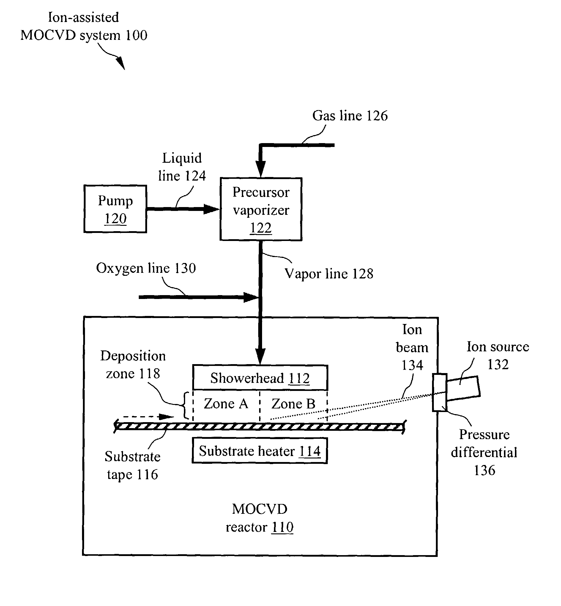
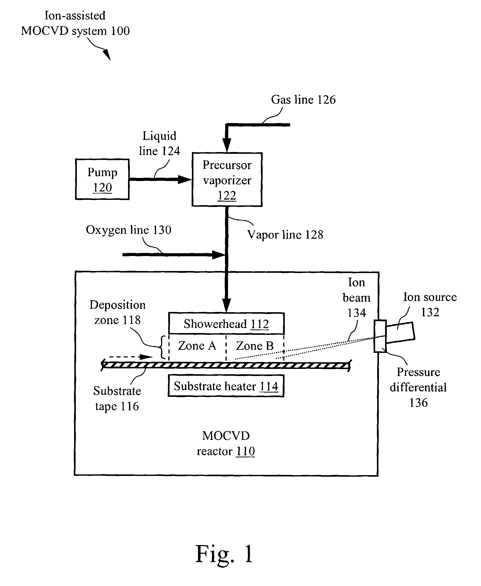
[0019]As the invention, FIG. 1 illustrates an ion-assisted MOCVD system 100 in accordance with the invention for producing high-current HTS-coated tapes by depositing HTS thick film with increased current capability. The ion-assisted MOCVD system 100 of the present invention includes a conventional MOCVD reactor 110, which is a vacuum-sealed deposition chamber in which an MOCVD process occurs, such as a cold-wall reactor that may be maintained at a pressure of, for example, 1.6 Torr.

[0020]The MOCVD reactor 110 houses a showerhead 112 located in close proximity to a substrate heater 114. A substrate tape 116 is positioned and translates (during operation) between the showerhead 112 and the substrate heater 114 within a deposition zone 118 formed along the length of the showerhead 112, i.e., the area in which the substrate tape 116 is exposed to the precursor vapors. Furthermore, multiple regions within the deposition zone 118 are established, for example, a zone A and a zone B as sho...

second embodiment

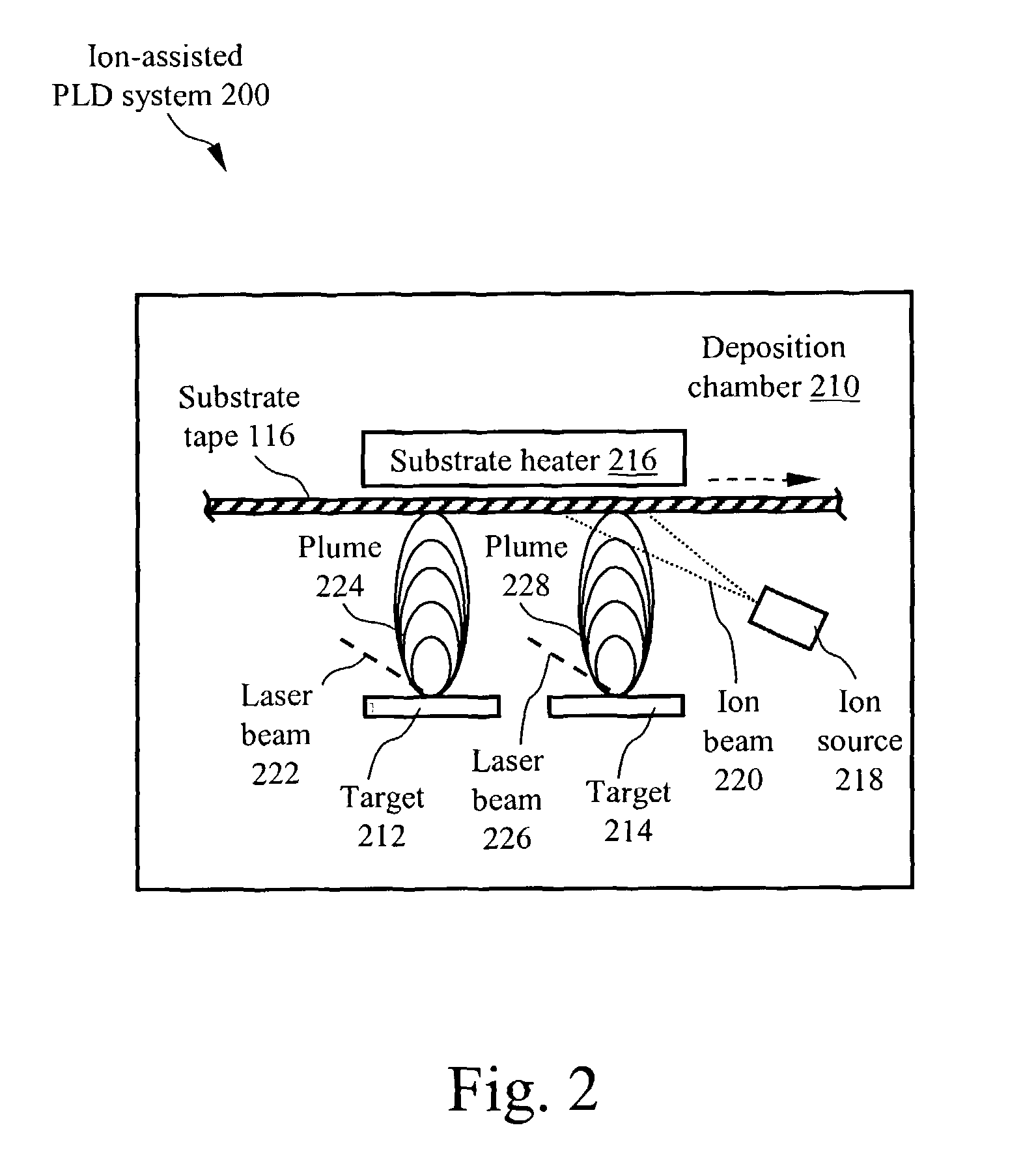
[0038]FIG. 2 illustrates the invention, an ion-assisted PLD system 200 for producing high-current HTS-coated tapes by depositing HTS thick film with increased current capability. The ion-assisted PLD system 200 of the present invention includes a conventional deposition chamber 210, which is a vacuum chamber designed specifically for pulsed laser deposition applications. An example of such a vacuum chamber is a 12- or 18-inch vacuum chamber commercially available by Neocera, [10000 Virginia Manor Road Beltsville, Md. 20705] although those skilled in the art will appreciate that a number of alternative vendors manufacture vacuum chambers in a variety of shapes and sizes. The deposition chamber 210 is maintained at a pressure of, for example, 200 mTorr. In this example, the deposition chamber 210 houses a first target 212 and a second target 214 that are located in close proximity to a substrate heater 216. The substrate tape 116 as described in FIG. 1 is positioned and translates (du...


PUM

PropertyMeasurementUnit
thicknessaaaaaaaaaa
thicknessaaaaaaaaaa
thicknessesaaaaaaaaaa

Abstract

An ion source impinging on the surface of the substrate to be coated is used to enhance a MOCVD, PVD or other process for the preparation of superconducting materials.

Description

FIELD OF THE INVENTION[0001]The present invention relates to the manufacture of thick film high-temperature superconductor (HTS) coated wire having increased current capability.BACKGROUND OF THE INVENTION[0002]In the past three decades, electricity has risen from 25% to 40% of end-use energy consumption in the United States. With this rising demand for power comes an increasingly critical requirement for highly reliable, high quality power. As power demands continue to grow, older urban electric power systems in particular are being pushed to the limit of performance, requiring new solutions.[0003]Wire forms the basic building block of the world's electric power system, including transformers, transmission and distribution systems, and motors. The discovery of revolutionary HTS compounds in 1986 led to the development of a radically new type of wire for the power industry; this discovery is the most fundamental advance in wire technology in more than a century.[0004]HTS-coated wire ...

Claims


Application Information

Patent Timeline
Patent Type & Authority Patents(United States)
IPC IPC(8): B05D5/12H01L39/24C23C14/00C23C14/08C23C14/22C23C14/28C23C16/40C23C16/48H10N60/01
CPCC23C14/087C23C14/22C23C14/28C23C16/408C23C16/486H01L39/2441H01L39/2448H10N60/0464H10N60/0521C23C14/46C23C14/08C23C14/26C23C14/14
Inventor SELVAMANICKAM, VENKATLEE, HEE-GYOUN
Owner SUPERPOWER INC
Learn More