Semiconductor device

a technology of semiconductor devices and semiconductors, applied in semiconductor devices, semiconductor/solid-state device details, electrical apparatus, etc., can solve the problems of decreasing the amount of current and increasing the breakdown voltage in this region, and achieve the effect of increasing the breakdown voltage in the boundary region, suppressing the thermal destruction resulting from increased temperature in this boundary region, and increasing the current density

Active Publication Date: 2014-04-01
MITSUBISHI ELECTRIC CORP
View PDF20 Cites 19 Cited by
  • Summary
  • Abstract
  • Description
  • Claims
  • Application Information

AI Technical Summary

Benefits of technology

[0013]According to the semiconductor device of one aspect of the present invention, while the amount of the current flowing through the active region of the diode can be ensured, an increase in the current density can be suppressed in the boundary region between the edge termination region and the diode active region, and also, thermal destruction resulting from increased temperature in this boundary region can be suppressed. In other words, the breakdown voltage in the boundary region is increased.
[0014]In addition to the above-described effects, the semiconductor device according to another aspect and still another aspect of the present invention allows a reduction in a forward voltage drop (VF) and suppression of the oscillation during recovery.

Problems solved by technology

In other words, the current concentration is reduced in the region in the vicinity of the guard ring in the OFF state, which causes an increase in the breakdown voltage in this region.
This causes a decrease in the density of carriers accumulated in the drift layer in the ON state, which may result in a decrease in the amount of the current that should essentially flow into the diode.

Method used


Image

  • Semiconductor device
  • Semiconductor device
  • Semiconductor device

Examples


first embodiment

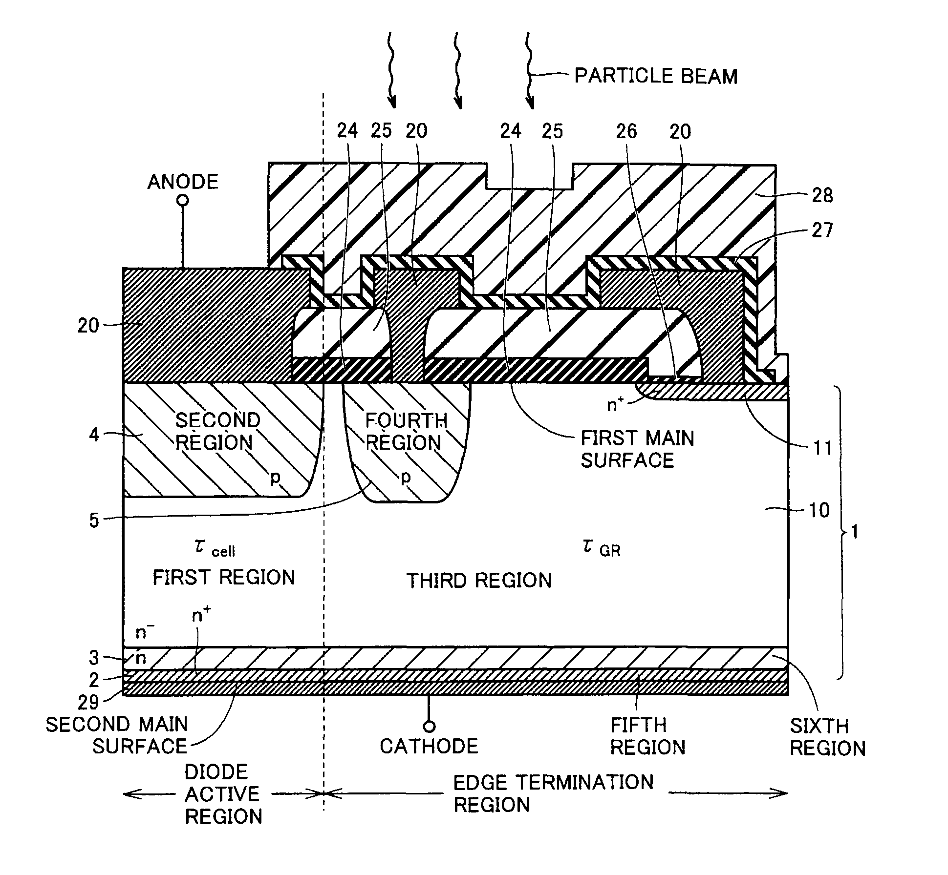
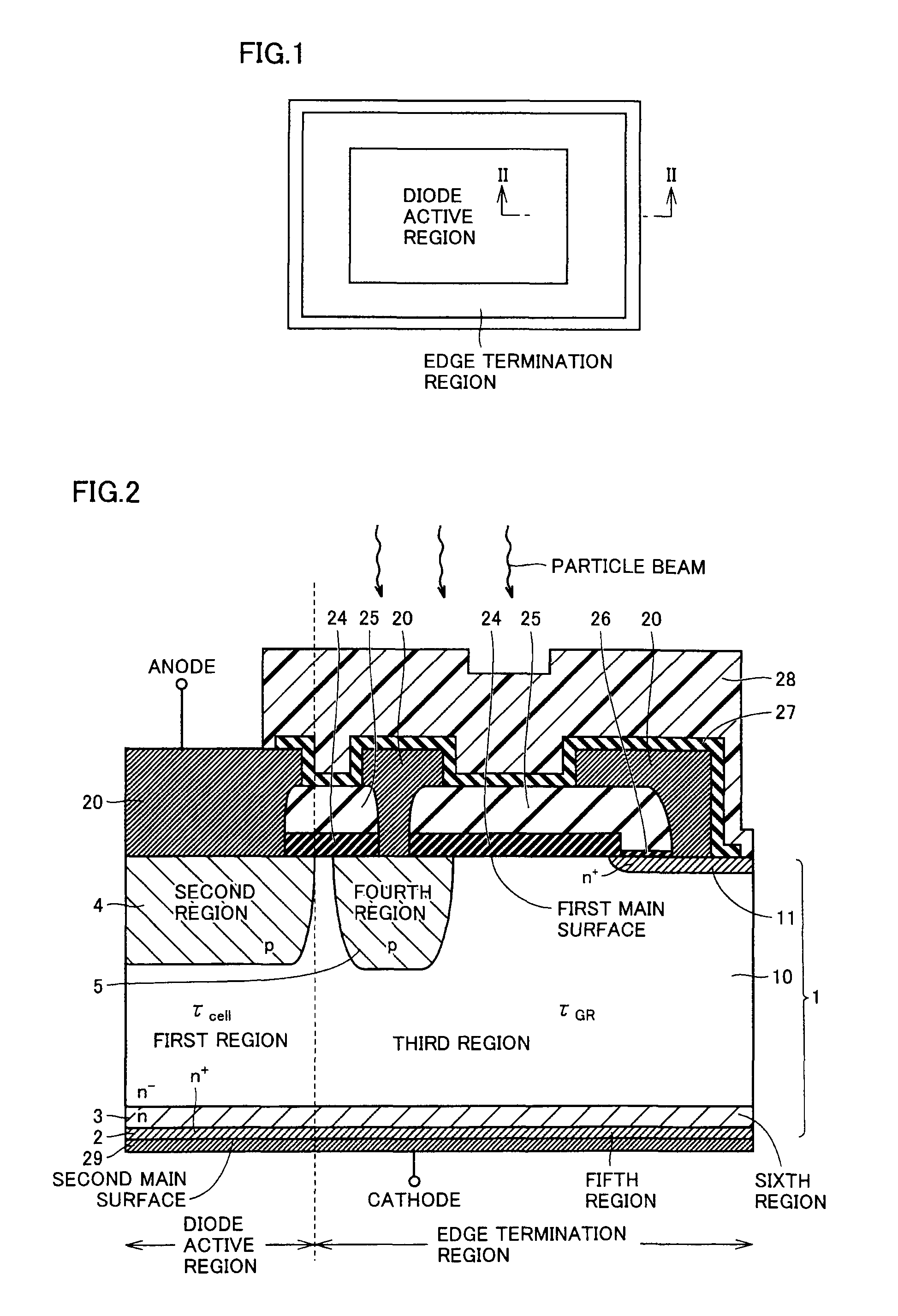
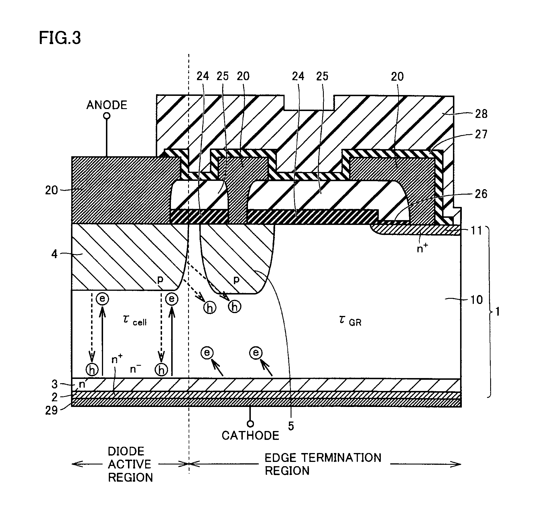
[0064]Referring to FIG. 1, the semiconductor device (diode) according to the present embodiment includes a diode active region and an edge termination region. The edge termination region surrounds the diode active region as seen in plan view.

[0065]FIG. 2 is a cross-sectional view taken along a line II-II in FIG. 1. Referring to FIG. 2, the semiconductor device according to Example 1 in the present embodiment includes a semiconductor substrate 1. Semiconductor substrate 1 is, for example, made of a single crystal of silicon, has the first main surface and the second main surface facing each other, and has the diode active region and the edge termination region as described above.

[0066]In the diode active region, a region (first region) of an n-type (first conductivity type) and a region (second region) of a p-type (second conductivity type) are joined to form a pn junction diode. Specifically, it includes an n− drift layer 10 (drift region), an n+ layer 2 (fifth region) and an n-type...

second embodiment

[0148]The semiconductor device according to the present embodiment is different in the anode configuration from the semiconductor device according to the first embodiment. The present embodiment will be hereinafter described.

[0149]Referring to FIG. 33, a p-type diffusion layer 8, an n-type diffusion layer 17, a trench structure 22, and a p+ diffusion layer 9 are formed on the anode side of the diode active region in the semiconductor device according to Example 1 of the present embodiment.

[0150]As with p-type regions 4 and 5, n-type diffusion layer 17 is a region of an n-type formed on the first main surface side of n− drift layer 10. P-type diffusion layer 8 is a region of a p-type formed on the first main surface side of n-type diffusion layer 17. P-type diffusion layer 8 and n-type diffusion layer 17 are formed also on the underside of n+ region 11 in the edge termination region. Trench structure 22 has a trench extending from the first main surface through p-type diffusion layer...

third embodiment

[0167]The semiconductor device according to the present embodiment is different in the configuration of the edge termination from the semiconductor device according to each of the first and second embodiments. The present embodiment will be hereinafter described.

[0168]Referring to FIGS. 36 to 41, the semiconductor device according to each of Examples 1 to 6 of the present embodiment is basically similar in configuration to the semiconductor device according to each Example of the first and second embodiments in FIGS. 15, 2, 7, 33, 34, and 35, respectively. It is to be noted that, on the anode side in the edge termination region in the semiconductor device according to each of Examples 1 to 6 of the present embodiment, a plurality of p-type regions 5 each as an edge termination are formed such that p-type regions 5 are arranged spaced apart from each other with respect to the first main surface of semiconductor substrate 1. The region having a plurality of edge terminations (guard ri...


PUM


Abstract

A semiconductor device includes a semiconductor substrate having a diode active region and an edge termination region adjacent to each other, a first region of a first conductivity type in the diode active region, a second region of a second conductivity type, a third region of the first conductivity type in the edge termination region, and a fourth region of the second conductivity type. The first region and the third region share a drift region of the first conductivity type. The first region and the third region share a fifth region of the first conductivity type. The drift region in the third region is greater in number of crystal defects per unit volume than the drift region in the first region in order that the drift region in the third region is shorter in carrier lifetime than the drift region in the first region.

Description

BACKGROUND OF THE INVENTION[0001]1. Field of the Invention[0002]The present invention relates to a semiconductor device, and particularly to a power semiconductor device of high breakdown voltage provided with a diode.[0003]2. Description of the Background Art[0004]An example of the power semiconductor device may include a power module of high breakdown voltage that can withstand a voltage, for example, greater than or equal to 600V. Such a power module may be equipped with an IGBT and a diode.[0005]For example, Japanese Patent Laying-Open No. 2009-283781 discloses a semiconductor device provided with a diode, in which an n-type semiconductor substrate has an anode formed on one main surface and a cathode formed on the other main surface. The anode is a p-type diffusion region and the cathode is formed of an n-type super-high concentration impurity layer and an n-type high concentration impurity layer. A guard ring is formed so as to surround this anode. A p-type diffusion region on...

Claims


Application Information

Patent Timeline
Patent Type & Authority Patents(United States)
IPC IPC(8): H01L29/02
CPCH01L2924/0002H01L29/402H01L23/3171H01L29/861H01L29/0619H01L2224/02166H01L2924/00H01L29/7811
Inventor NAKAMURA, KATSUMI
Owner MITSUBISHI ELECTRIC CORP
Why Eureka
Try Eureka