Semiconductor package

a technology of semiconductors and components, applied in the field of semiconductor devices, can solve the problems of high space requirements and high routing effort, and achieve the effect of facilitating the addition of additional electronic components

Active Publication Date: 2015-03-17
BIOTRONIK SE & CO KG
View PDF2 Cites 4 Cited by
  • Summary
  • Abstract
  • Description
  • Claims
  • Application Information

AI Technical Summary

Benefits of technology

[0009]It is of advantage that the present invention allows for a standardized test point methodology. Thus, module-level test systems for both engineering and production uses can be designed for a simplified header / socket model with minimal tooling change between testing different models.
[0022]According to an advantageous embodiment, the test portal may be arranged at an external surface, e.g., at the top surface and / or at the side walls, thus providing easy accessibility for both for both engineering and production uses. Routing for top-side test points also facilitates the addition of additional electronic components such as, for example, decoupling caps on top of or within the BGA package. A decoupling cap is a specific type of small electronic component. However, any electronic component small enough to be mounted within, or on top of, the package could be used without departing from the spirit and scope of the present invention.

Problems solved by technology

In hybrid electronics modules, all test points must be routed to metalized points in one of the module surfaces, which results in a routing effort as well as a high space requirement.

Method used


Image

  • Semiconductor package
  • Semiconductor package
  • Semiconductor package

Examples


Embodiment Construction

[0037]In the drawings, like elements are referred to with equal, or the same, reference numerals. The drawings are merely exemplary schematic representations, and are not intended to portray specific parameters of the present invention. Moreover, the drawings are intended to depict only typical exemplary embodiments of the present invention and, therefore, should not be considered as limiting the scope of the present invention.

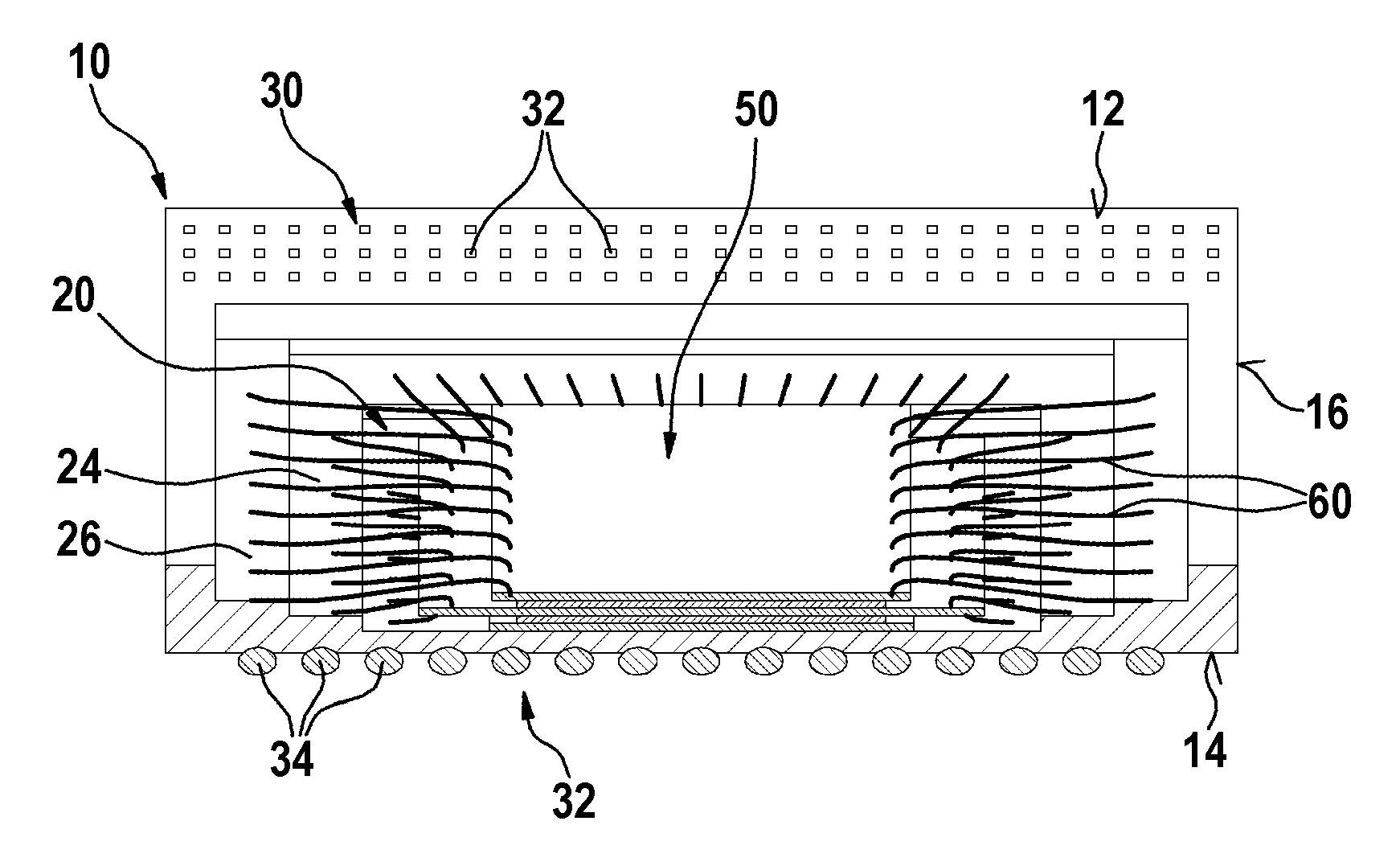
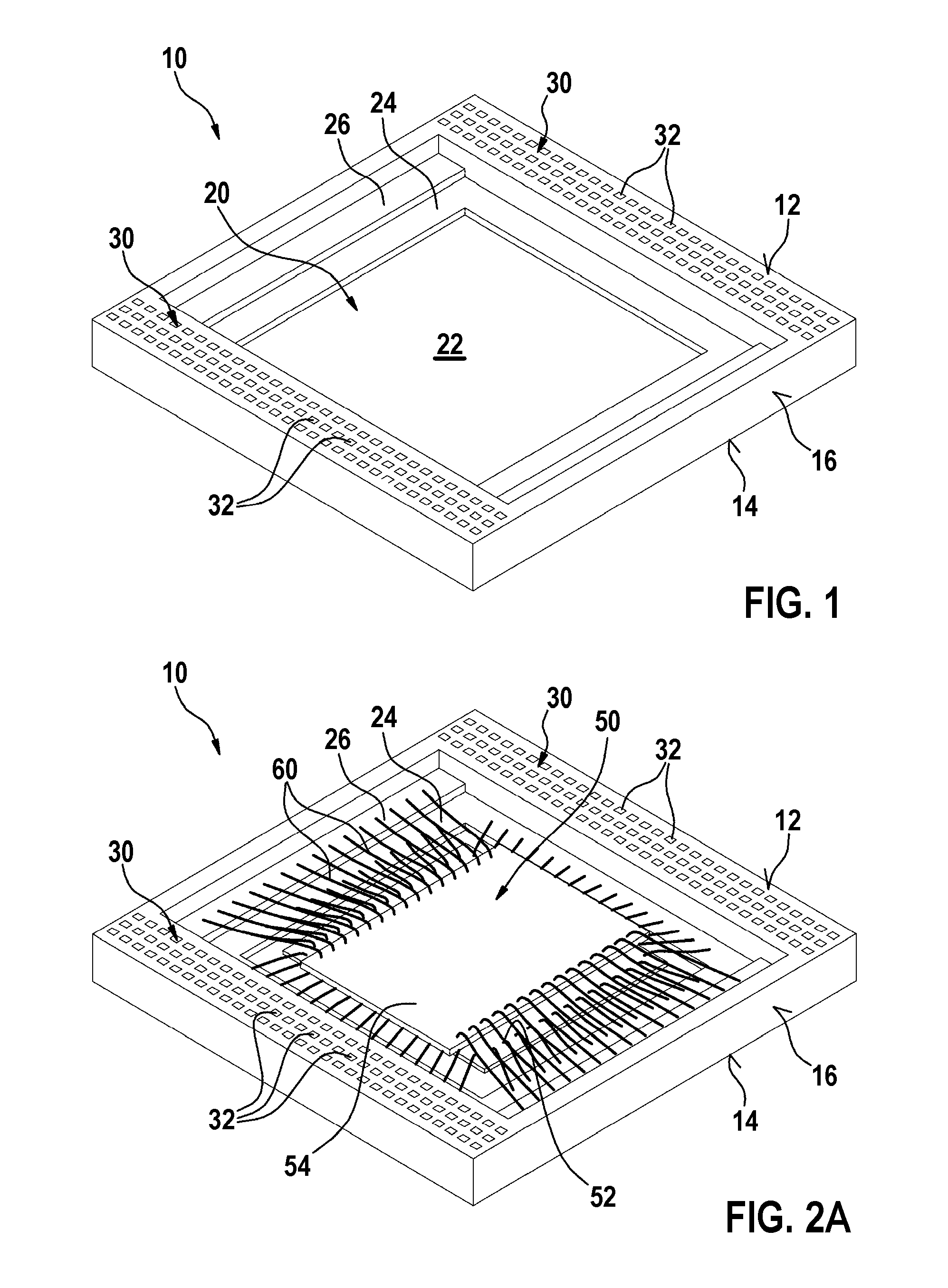
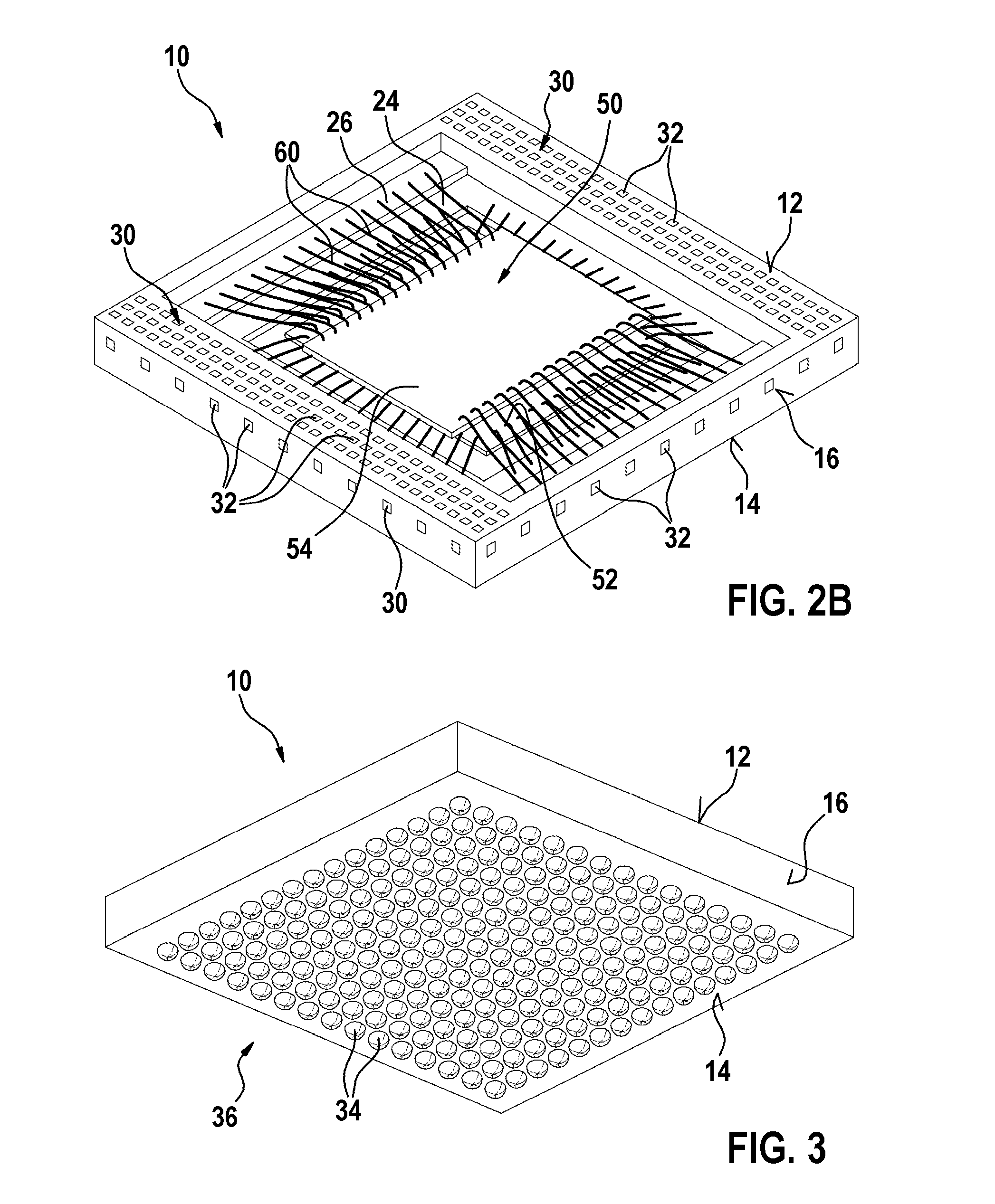
[0038]FIG. 1 depicts an exemplary embodiment of a carrier 10 according to the present invention. The carrier 10 has a top surface 12 and a bottom surface 14 separated by side walls 16. The carrier 10 is advantageously embodied as a multi-layered printed circuit board assembly comprising a seat 20 for mounting an electric component 50 such as, for example, a semiconductor die.

[0039]A first 24 and a second 26 terminal region for electrically connecting the component 50 to the carrier 10 are arranged in a recess 22, which includes the seat 20. The first and secon...


PUM


Abstract

A semiconductor package and a carrier for a semiconductor package are provided, the carrier having a top surface and a bottom surface separated by side walls. The carrier includes a seat for a component, and at least one terminal region for electrically connecting the component to the carrier when mounted to the seat, wherein a test portal is arranged at an outer surface of the carrier, and wherein one or more routing paths are arranged in the carrier for routing one or more electrical contacts arranged at the carrier to the test portal.

Description

RELATED APPLICATION[0001]This patent application claims the benefit of U.S. Provisional Patent Application No. 61 / 497,966, filed on Jun. 17, 2011, the disclosure of which is hereby incorporated by reference in its entirety.TECHNICAL FIELD[0002]The present inventive disclosure relates to a semiconductor device and, more specifically, to a semiconductor package.BACKGROUND[0003]It is known in the art to provide test points on hybrid electronics modules. In hybrid electronics modules, all test points must be routed to metalized points in one of the module surfaces, which results in a routing effort as well as a high space requirement.[0004]The present invention is directed toward overcoming one or more of the above-identified problems.[0005]It is an object of the present invention to provide a carrier for a semiconductor package with reduced space requirements for routing test points to the semiconductor module.[0006]It is a further object of the present invention to provide a semicondu...

Claims


Application Information

Patent Timeline
Patent Type & Authority Patents(United States)
IPC IPC(8): H01L23/02H01L23/00H01L23/13H01L23/498H01L25/065
CPCH01L23/13H01L23/49805H01L23/49838H01L2924/15313H01L24/48H01L24/49H01L2224/32145H01L2224/32225H01L2224/48091H01L2224/48227H01L2224/49171H01L2224/73265H01L2225/06596H01L2924/15312H01L2924/15311H01L2924/15156H01L2225/06562H01L2225/0651H01L2224/49175H01L2224/48105H01L25/0657H01L23/49816H01L2924/00014H01L2924/00012H01L2924/00H01L24/73H01L2224/45099H01L2224/45015H01L2924/207
Inventor BIRGE, ADAMPICKUP, KEVINPRIMAVERA, ANTHONY A.
Owner BIOTRONIK SE & CO KG
Why Eureka
Try Eureka