Sub-block disabling in 3D memory
a technology of 3d memory and subblocks, applied in the field of 3d memory subblock disabling, can solve the problems of large amounts of memory becoming unusable by users, blocks may also become defective during the lifetime of a memory device, and may thereafter be unusabl
- Summary
- Abstract
- Description
- Claims
- Application Information
AI Technical Summary
Benefits of technology
Problems solved by technology
Method used
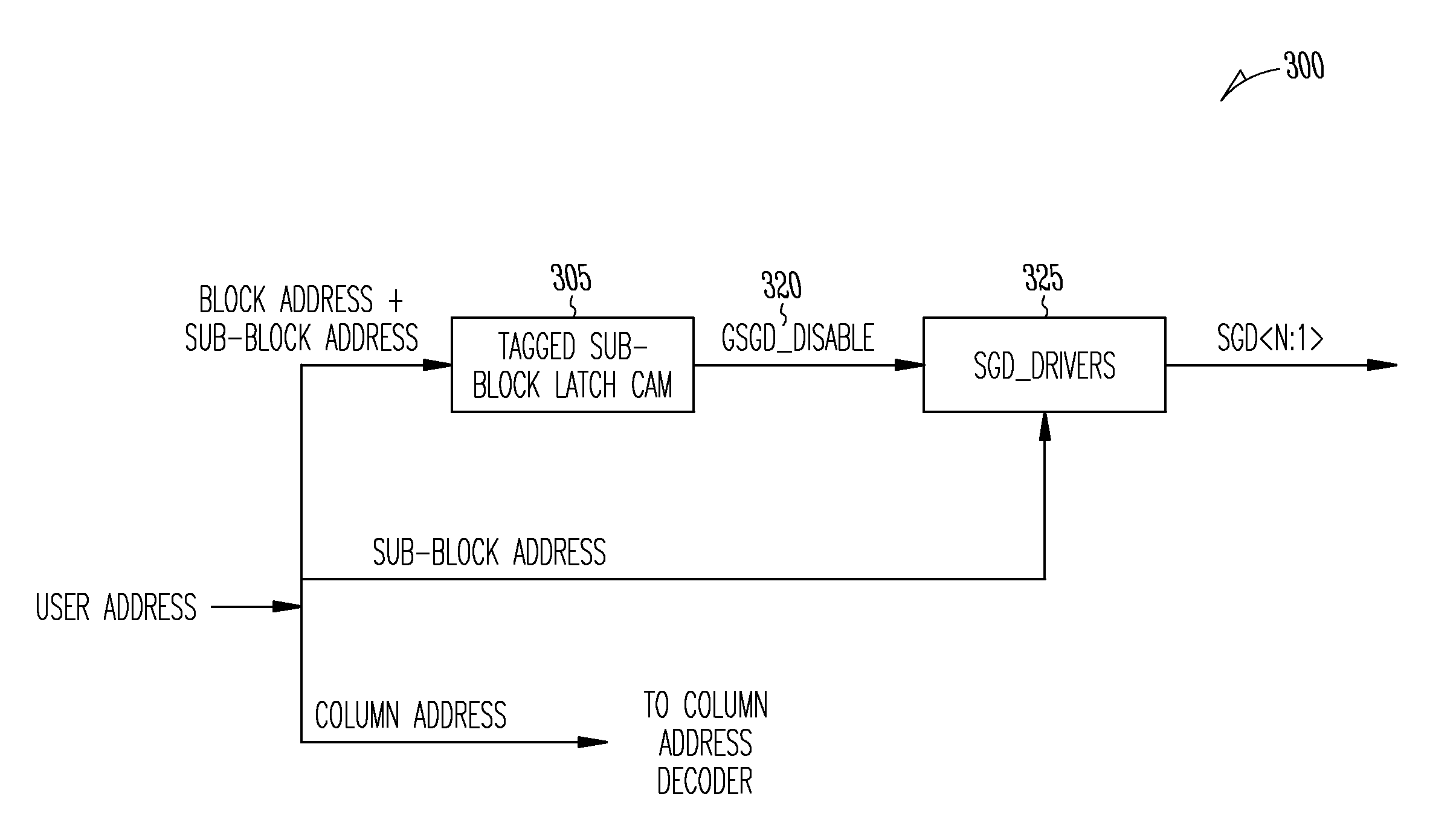
Image


Examples
Embodiment Construction
[0010]A block of memory cells according to various embodiments may function as a block of memory cells in a memory device such as a NOT AND (NAND) memory device. Memory cells may be arranged in a three-dimensional manner.
[0011]FIG. 1 shows a block diagram of an apparatus in the form of a memory device 100. The memory device 100 may include two or more blocks 110-1, 110-2. Each block 110-1, 110-2 may include two or more sub-blocks 120-1 through 120-n. The two or more sub-blocks 120-1 through 120-n may each comprise a vertical string 130. The vertical string 130 may include a number of memory cells 132-0 through 132-15. In the illustrative example, the vertical string 130 includes 16 memory cells. However, it will be understood that the vertical string 130 may include any number of memory cells. The memory cells 132-0 through 132-15 may be coupled in series.
[0012]The vertical string 130 may include a source select gate (SGS) transistor 140-1, which is sometimes also referred to herein...
PUM
 Abstract
Description
Claims
Application Information
 - R&D
- Intellectual Property
- Life Sciences
- Materials
- Tech Scout
- Unparalleled Data Quality
- Higher Quality Content
- 60% Fewer Hallucinations
Browse by: Latest US Patents, China's latest patents, Technical Efficacy Thesaurus, Application Domain, Technology Topic, Popular Technical Reports.
© 2025 PatSnap. All rights reserved.Legal|Privacy policy|Modern Slavery Act Transparency Statement|Sitemap|About US| Contact US: help@patsnap.com